Gallium nitride based high electron mobility transistor with composite metal gate

A high electron mobility, gallium nitride-based technology, applied in the field of gallium nitride-based high electron mobility transistors, can solve problems such as increasing the complexity of device applications, and achieve increased complexity, improved transmission efficiency, and insufficient compensation Effect

Active Publication Date: 2013-12-25
UNIV OF ELECTRONICS SCI & TECH OF CHINA
View PDF5 Cites 6 Cited by
  • Summary
  • Abstract
  • Description
  • Claims
  • Application Information

AI Technical Summary

Problems solved by technology

But on the other hand, double-gate field effect transistors may increase the gate capacitance C of the device g , on the contrary, it will have a negative impact on the frequency characteristics of the device, and change the original three-terminal device into a four-terminal device, which increases the complexity of the device application

Method used


Image

  • Gallium nitride based high electron mobility transistor with composite metal gate
  • Gallium nitride based high electron mobility transistor with composite metal gate
  • Gallium nitride based high electron mobility transistor with composite metal gate

Examples


Embodiment

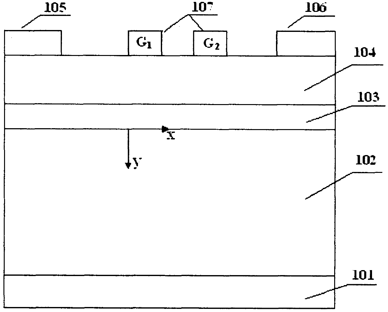
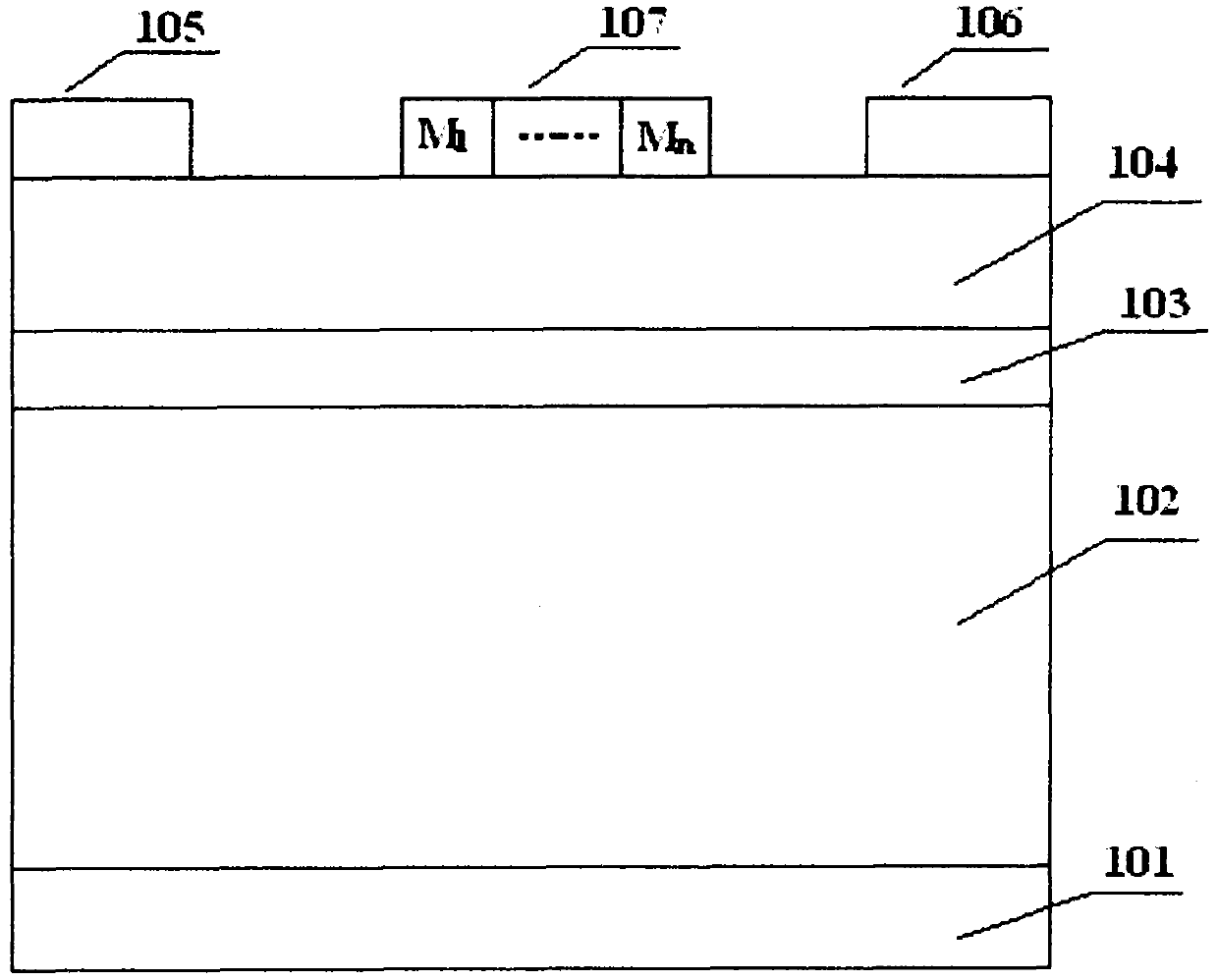
[0043] In the present invention, as image 3 As shown, the gate 107 is a composite metal gate, and each gate metal (M 1 , M 2 ,...,M n , n≥2) can be platinum (Pt), gold (Au), nickel (Ni), titanium (Ti), silver (Ag), aluminum (A1), chromium (Cr), cadmium (Cd), molybdenum (Mo ) etc.; the work function of the gate metal (WF 1 , WF 2 ,...,WF n , n≥2) ranges from 4 to 7eV, and satisfies the relationship of decreasing successively along the direction from the source 105 to the drain 106; each metal length (L g1 , L g2 ,...,L gn , n≥2) are all 1 nm to 20 μm, and the total length of the grid is 2 nm to 20 μm.

[0044] In order to verify the effect of the composite metal gate of the present invention, the gallium nitride-based high electron mobility using single gate (SG), double gate (DG), double metal composite gate (DMCG) and triple metal composite gate (TMCG) High-rate transistor devices are simulated and compared. In this example, Al x In y Ga z In N, x=0.26, y=0, z=0...


PUM

PropertyMeasurementUnit
lengthaaaaaaaaaa
lengthaaaaaaaaaa
lengthaaaaaaaaaa

Abstract

The invention relates to a gallium nitride based high electron mobility transistor with a composite metal gate. The gallium nitride based high electron mobility transistor comprises a substrate, a gallium nitride buffer layer, an aluminum nitride inserting layer, an aluminum-indium-gallium-nitrogen barrier layer, and a source electrode, a drain electrode and a grid electrode on the aluminum-indium-gallium-nitrogen barrier layer, wherein the source electrode and the drain electrode form ohmic contact with the aluminum-indium-gallium-nitrogen barrier layer; the grid electrode and the aluminum-indium-gallium-nitrogen barrier layer form Schottky contact; the grid electrode on the aluminum-indium-gallium-nitrogen barrier layer is formed by connecting more than two metals with different work functions. Through the utilization of the influence of a step barrier shielding drain potential formed between the grid metals with different work functions on device channels, the Drain Induced Barrier Lowering (DIBL) effect is inhibited, and the SCEs (Short Channel Effects) of deep submicron gallium nitride based high electron mobility transistor are improved, thus the current gain cut-off frequency fT is improved.

Description

technical field [0001] The invention relates to the field of semiconductor devices, in particular to a gallium nitride-based high electron mobility transistor with a composite metal gate. Background technique [0002] Gallium nitride-based high electron mobility transistor (High Electron Mobility Transistor, HEMT) not only has gallium nitride (GaN) material with large bandgap, high critical breakdown electric field, high electron saturation drift velocity, high temperature resistance, radiation resistance and good Excellent properties such as chemical stability, and GaN materials can form a two-dimensional electron gas (2DEG) channel with high concentration and high mobility with materials such as aluminum gallium nitride (A1GaN), so it is especially suitable for high voltage, high power and high temperature It is one of the most potential transistors for power electronics applications. [0003] figure 1 It is a cross-sectional view of the structure of a GaN-based high ele...

Claims


Application Information

Patent Timeline
Patent Type & Authority Applications(China)
IPC IPC(8): H01L29/10H01L29/778
Inventor 杜江锋严慧刘斌尹成功黄思霓罗杰白智元陈南庭于奇
Owner UNIV OF ELECTRONICS SCI & TECH OF CHINA
Why Eureka
Try Eureka