

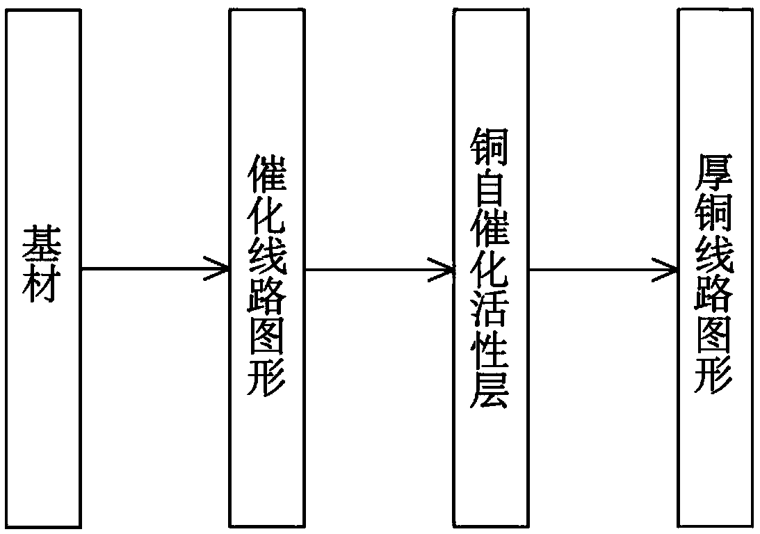
Printed circuit addition manufacturing method based on copper autocatalysis and chemical copper plating
A printed circuit and electroless copper plating technology, which is applied in the fields of printed circuit manufacturing, printed circuit, electrical components, etc., can solve the problems such as difficult to realize the preparation of thick copper wires, poor conductivity of conductive patterns, easy shrinkage and deformation of wires, etc., to achieve improved Good conductivity and practicability, good density and uniformity, and good conductivity
- Summary
- Abstract
- Description
- Claims
- Application Information
AI Technical Summary
Problems solved by technology
Method used
Image

Examples
specific Embodiment approach 1
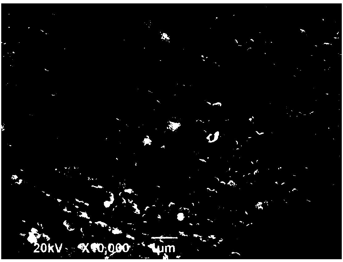
[0027] Catalyst for electroless copper plating with copper:
[0028] Dissolve 0.016mol of copper sulfate in 44mL of deionized water, then add 1mL of glycerin and 5mL of isopropanol to adjust the viscosity of the solution to 2.1mPa·s and the surface tension to 32mN / m to obtain copper ion ink; 0.03mol of sodium hydroxide Dissolve in 35mL deionized water, then dissolve 0.034mol sodium borohydride in the above sodium hydroxide solution, then add 5mL glycerol and 10mL isopropanol to adjust the solution viscosity to 2.3mPa·s and surface tension to 30mN / m, namely Get reducing agent ink. Load the two inks into the printer's two ink cartridges, and the printer is ready to go.
[0029] The polyimide (PI) substrate was washed with water and dried to prepare a substrate pretreatment solution, which contained: 1.5 mol / L sodium hydroxide, 0.2 mol / L sodium carbonate, and 0.03 mol / L trisodium phosphate. It has both degreasing and roughening effects on polyimide substrates. Heat the solution...
specific Embodiment approach 2
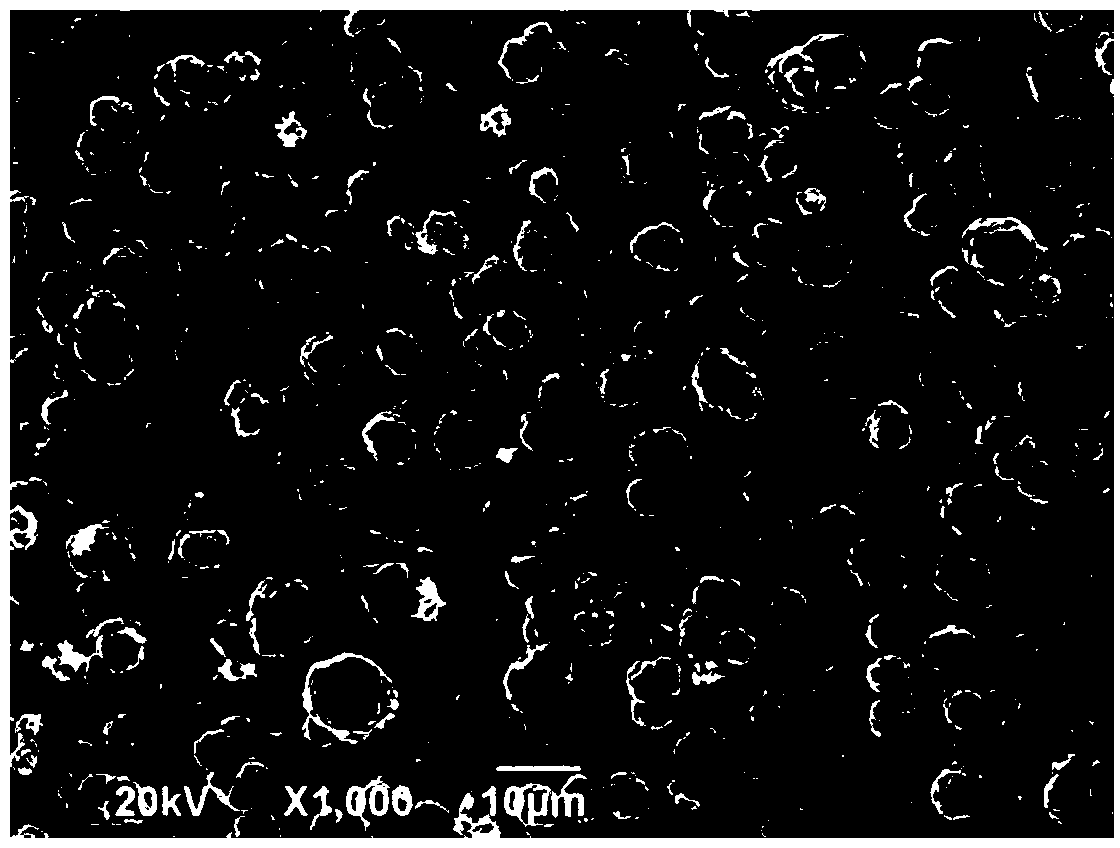
[0033] Catalyst for electroless copper plating with silver:
[0034] Dissolve 0.02 mol of silver nitrate in 30 mL of deionized water, then add 10 mL of ethanol, 5 mL of ethylene glycol and 5 mL of n-propanol to adjust the viscosity of the solution to 2.7 mPa·s and the surface tension to 32 mN / m to obtain a silver ion catalytic ink. Ink is loaded into the printer cartridges and the printer is ready to go.
[0035] The polyimide base material is selected and processed according to the method in Embodiment 1, and the silver ion ink is printed on the base material, and then treated after curing to be plated.
[0036] Prepare the first step copper plating solution, wherein the concentration of each component is: copper sulfate 0.04mol / L, aminotriacetic acid 0.16mol / L, sodium hydroxide 0.25mol / L and formaldehyde 0.16mol / L, 2-mercaptobenzothiazole 10mg / L, the pH of the plating solution is 13, heat the constant temperature plating solution in a water bath at 45°C, immerse the substra...
PUM
| Property | Measurement | Unit |
|---|---|---|
| Thickness | aaaaa | aaaaa |
| Resistivity | aaaaa | aaaaa |
| Resistivity | aaaaa | aaaaa |
Abstract
Description
Claims
Application Information