


Quick Research
Generate reliable direction feasibility study reports for your R&D in just a few steps.

Technical Q&A
Discover and master advanced knowledge NOW. Basics, ideas, possibilities, all at once.

Find Solutions
As an expert in R&D theories, this can generate solutions to your technical problems instantly.

Evaluate Feasibility
Analyze your overall solution with one click, know your potential R&D risks in advance.

Monitor Landscape
Get weekly tech updates, stay abreast of the latest tech innovations and key insights.
D-A type polymer semiconductor material and preparation method and application thereof
A polymer, D-A technology, applied in semiconductor/solid-state device manufacturing, semiconductor devices, electric solid-state devices, etc., can solve the problem of unreported preparation performance of related polymers, achieve simple preparation and testing, expand the scope of application, repeatable good effect
- Summary
- Abstract
- Description
- Claims
- Application Information
AI Technical Summary
Problems solved by technology
Method used
Image

Examples
Embodiment 1
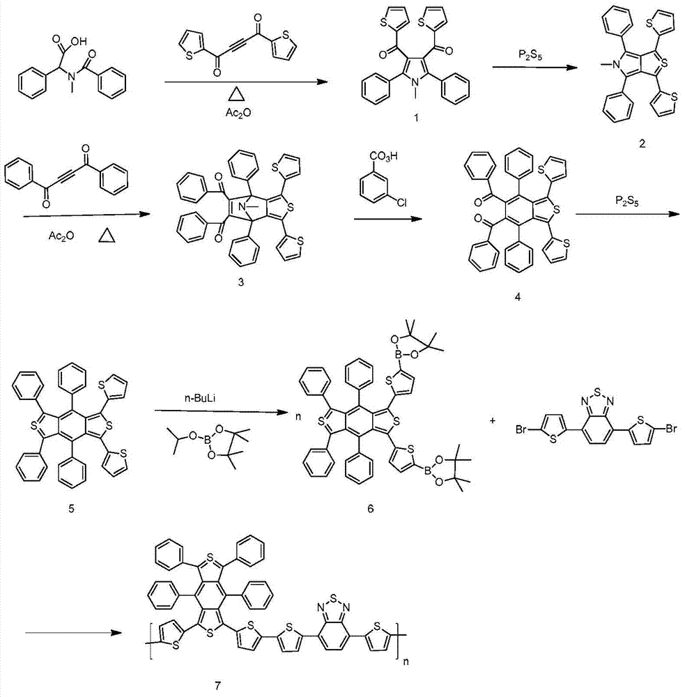
[0064] Example 1, Preparation of poly 1,2,3,4-tetraphenyl-5,6-dithienyldithienoabenzo-4,7-dithiophenebenzothiadiazole (PTPTDTP-DTBTD)
[0065] (1) Synthesis of 1-methyl-2,5-diphenyl-3,4-dithienylpyrrole (product shown in formula 7)
[0066] In a 150mL two-necked flask, vacuum argon. Then add 80mL of glacial acetic acid and 2.69g (10mmol) of N-methyl-N-benzoylphenylglycine in sequence, stir at room temperature for 30min, then add 2.64g (11mmol) of 1,2-dithienoylacetylene dropwise, heat up to reflux and stir 5h, terminate the reaction. Wash with water and saturated sodium bicarbonate solution successively, and filter to obtain the compound represented by formula 1, which is 3.85 g of a tan product (yield 84.7%).
[0067] (2) Synthesis of N-methyl-2,5-diphenyl-3,4-dithienylthienopyrrole (compound shown in formula 2)
[0068] In a 250mL two-necked flask, vacuum argon. Then 120 mL of benzene and 4.51 g (10 mmol) of 1-methyl-2,5-diphenyl-3,4-dithienylpyrrole were added successiv...
Embodiment 2
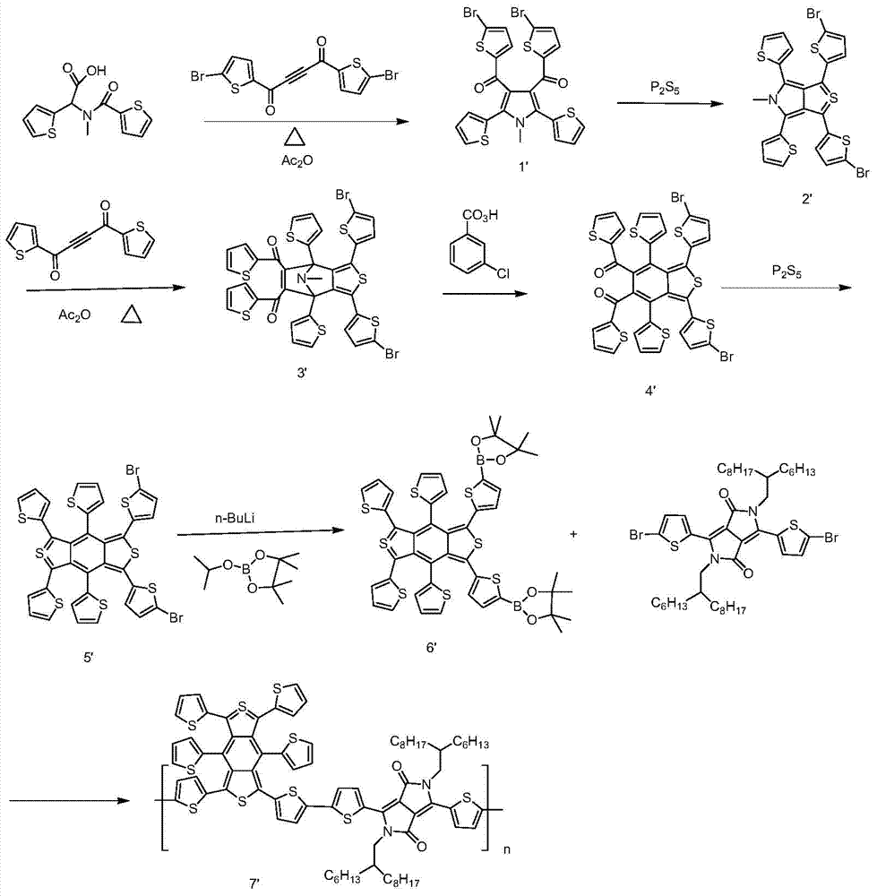
[0080] Example 2, Preparation of poly 1,2,3,4-tetrathienyl-5,6-dithienyldithienoabenzo-3,6-dithiophenepyrrolopyrrole diketone (PHTDTP-BTDPP)
[0081] (1) Synthesis of 1-methyl-2,5-dithienyl-3,4-di(2'-bromo)thienylpyrrole (compound represented by formula 1')
[0082] In a 150mL two-necked flask, vacuum argon. Then add 80mL of glacial acetic acid and 2.81g (10mmol) of N-methyl-N-thienoylphenylglycine in sequence, stir at room temperature for 30min and then add 4.44g (11mmol) of 1,2-di(2'-bromo)thienoylacetylene dropwise. ), heated to reflux and stirred for 5h to terminate the reaction. Wash with water and saturated sodium bicarbonate solution successively, and filter to obtain the compound represented by formula 1', which is 5.1 g of a tan product (yield 85%).
[0083] (2) Synthesis of N-methyl-2,5-dithienyl-3,4-di(2'-bromo)thienylthienopyrrole (compound represented by formula 2')
[0084] In a 250mL two-necked flask, vacuum argon. Then add 120mL of benzene and 6.05g (10mmol...
Embodiment 3
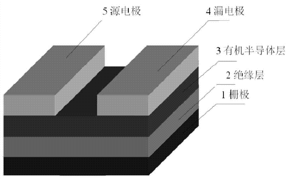
[0096] Embodiment 3, the preparation of PTPTDTP organic field effect transistor device
[0097] Silicon wafer cleaning: Cut a silicon wafer with an inorganic insulating layer of silicon dioxide on one side into small pieces of appropriate size, put it in a beaker, add a mixed solvent of hydrogen peroxide and concentrated sulfuric acid with a ratio of about 3:7, and heat it in an electric furnace to boil for about 40 Minutes, pour off the solvent acid solution, rinse off the residual concentrated sulfuric acid and hydrogen peroxide with deionized water, then use deionized water and isopropanol to sonicate for about 10 minutes, and finally blow dry quickly with nitrogen.
[0098] Device preparation: get the silicon wafer with 300nm silicon dioxide on one side after cleaning, then deposit the PTPTDTP prepared in Example 1 on the other side by spin coating method, the solution used is the toluene solution of 2mg / ml, and the rotating speed is 3000 rpm, The thickness of the organic ...
PUM
| Property | Measurement | Unit |
|---|---|---|
| Thickness | aaaaa | aaaaa |
| Thickness | aaaaa | aaaaa |
Abstract
Description
Claims
Application Information
 - R&D Engineer
- R&D Manager
- IP Professional
- Industry Leading Data Capabilities
- Powerful AI technology
- Patent DNA Extraction
Browse by: Latest US Patents, China's latest patents, Technical Efficacy Thesaurus, Application Domain, Technology Topic, Popular Technical Reports.
© 2024 PatSnap. All rights reserved.Legal|Privacy policy|Modern Slavery Act Transparency Statement|Sitemap|About US| Contact US: help@patsnap.com