Method for manufacturing Pt resistor temperature sensor

A manufacturing method and technology of resistance temperature, applied to thermometers, thermometers using directly heat-sensitive electric/magnetic elements, instruments, etc., can solve the problems of slow ion beam etching rate, difficulty in reducing preparation efficiency and processing cost, etc.

Inactive Publication Date: 2014-01-01
BEIJING INSTITUTE OF TECHNOLOGYGY
View PDF6 Cites 7 Cited by
  • Summary
  • Abstract
  • Description
  • Claims
  • Application Information

AI Technical Summary

Problems solved by technology

Usually, the thickness of Pt metal is about 2 μm, but the problem with the current process is that the ion beam etching rate is very slow, and i

Method used


Image

  • Method for manufacturing Pt resistor temperature sensor

Examples


Embodiment 1

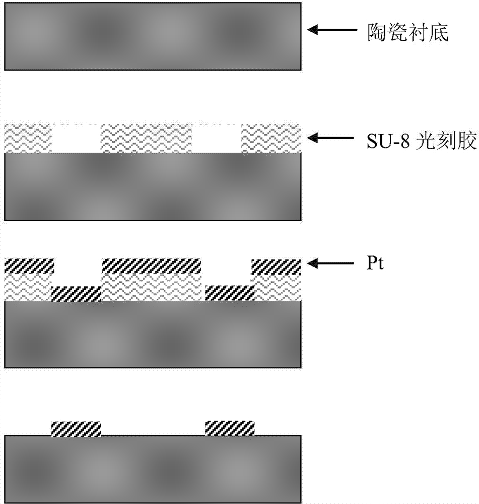
[0018] A method for manufacturing a Pt resistance temperature sensor, comprising the following steps:

[0019] (1) Clean a ceramic substrate of a certain size (such as 3 inches) with absolute ethanol (MOS grade) and deionized water in sequence, then dry it, and then evaporate HMDS (a coupling agent) on the ceramic substrate.

[0020] (2) Apply SU-82025 (a type of SU-8 glue) photoresist to the processed ceramic substrate by spin coating method, with a thickness of 5 μm to 10 μm.

[0021] (3) Pre-bake the photoresist on a hot plate under the conditions of 65°C / 3min and 95°C / 5min.

[0022] (4) Expose in a lithography machine with a UV light source, and the exposure meter is 150mJ / cm 2 .

[0023] (5) After-baking on a hot plate, the conditions are 65°C / 1min, 95°C / 5min.

[0024] (6) Develop with SU-8 special developer, and use O 2 Plasma to remove the bottom film.

[0025] (7) Put the photolithographically completed ceramic substrate into a magnetron multi-target sputtering ma...

Embodiment 2

[0029] (1) Use a ceramic substrate of a certain size (such as 3 inches) with H 2 SO 4 +H 2 o 2 , deionized water, and then dried, and then evaporated HMDS (a coupling agent) on the ceramic substrate.

[0030] (2) Apply SU-82025 (a type of SU-8 glue) photoresist to the processed ceramic substrate by spraying glue, with a thickness of 5 μm to 10 μm.

[0031] (3) Pre-bake the photoresist on a hot plate under the conditions of 65°C / 3min and 95°C / 5min.

[0032] (4) Expose in a lithography machine with a UV light source, and the exposure meter is 150mJ / cm 2 .

[0033] (5) After-baking on a hot plate, the conditions are 65°C / 1min, 95°C / 5min.

[0034] (6) Develop with SU-8 special developer, and use O 2 Plasma to remove the bottom film.

[0035] (7) Put the electron beam evaporation equipment above to obtain the ceramic substrate Pt metal with a thickness of about 2 μm.

[0036] (8) Put the ceramic substrate obtained above into a NaOH salt bath furnace at high temperature to ...


PUM

PropertyMeasurementUnit
Thicknessaaaaaaaaaa
Thicknessaaaaaaaaaa

Abstract

The invention discloses a method for manufacturing a Pt resistor temperature sensor. The method comprises the following steps that firstly, a ceramic substrate is coated with SU-8 photoresist, and a microstructural image is formed based on photolithography; secondly, by the adoption of the magnetron sputtering method, Pt metal is deposited on the ceramic substrate generated after photolithography is completed; thirdly, the ceramic substrate obtained in the second step is ablated in the oxygen atmosphere or placed into a salt bath so that the SU-8 photoresist can be removed; fourthly, a Pt metal microstructural image which is deposited on the ceramic substrate is obtained finally. According to the method for manufacturing the Pt resistor temperature sensor, the characteristic of good heat resistance of the SU-8 photoresist is utilized, the Pt resistor temperature sensor is manufactured by the adoption of the stripping technology, the technology is simple and easy to conduct, and cost is greatly reduced.

Description

technical field [0001] The invention relates to sensor manufacturing technology, in particular to a manufacturing method of a Pt resistance temperature sensor. Background technique [0002] Pt metal is particularly suitable for manufacturing temperature sensors due to its excellent temperature characteristics. The current method of manufacturing Pt resistance temperature sensor is mainly to use magnetron sputtering method to obtain Pt metal film, then apply glue on the Pt metal film, photolithography, and then use photoresist as a mask to etch with ion beam etching Figure out the Pt metal microstructure pattern. Usually, the thickness of Pt metal is about 2 μm, but the problem of the current process method is that the ion beam etching rate is very slow, and it takes 3 to 4 hours to etch Pt metal with a thickness of 2 μm, which makes it difficult to reduce the production efficiency and processing cost. Contents of the invention [0003] In order to overcome the deficienci...

Claims


Application Information

Patent Timeline
IPC IPC(8): G01K7/18
Inventor 李建华徐立新卢冲赢
Owner BEIJING INSTITUTE OF TECHNOLOGYGY
Why Eureka
Try Eureka