Enhanced radiation three-dimensional packaging structure and packaging method for same

A three-dimensional packaging and packaging method technology, applied in the direction of semiconductor/solid-state device components, semiconductor devices, electrical components, etc., can solve the problems of decreased heat transfer performance, high technical requirements, difficult application and promotion, etc. The effect of high integration, enhanced heat transfer and heat dissipation

Inactive Publication Date: 2014-01-01
PEKING UNIV
View PDF4 Cites 30 Cited by
  • Summary
  • Abstract
  • Description
  • Claims
  • Application Information

AI Technical Summary

Problems solved by technology

[0005] To remove extremely high heat at the device scale of millimeter or even nanometer, the traditional heat dissipation technology of electronic equipment is no longer applicable: the heat flux density of convection, radiation, conduction and other natural cooling heat dissipation does not exceed 0.155W / cm 2 ;The heat flux density of metal thermal vias and air cooling does not exceed 10W / cm 2 , advanced jet cooling technology can be used for 100W / cm 2 working environment, but the technical requirements are high, and the application and promotion are difficult; heat pipe cooling can be used for heat flux density greater than 100W / cm 2 The heat dissipation of the device can be manufactured into a product with a small volume and a very light weight, but limited by the working limit of heat flux density, flow resistance, capillary pressure difference, etc., the heat transfer performance will decrease after a period of use; thermoelectric cooling uses semiconductor materials (such as Bi 2 Te 3 ) Peltier effect, heat is absorbed and released at both ends of the galvanic couple, no noise and vibration, small size, compact structure, easy operation and maintenance, no refrigerant required, and the cooling capacity and cooling speed can be adjusted by changing the current size, But low efficiency and high cost

Method used


Image

  • Enhanced radiation three-dimensional packaging structure and packaging method for same
  • Enhanced radiation three-dimensional packaging structure and packaging method for same

Examples


Embodiment Construction

[0031] The present invention will be further described through the embodiments below in conjunction with the accompanying drawings.

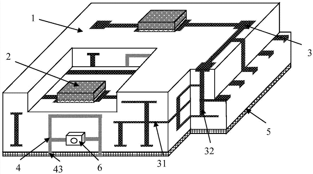
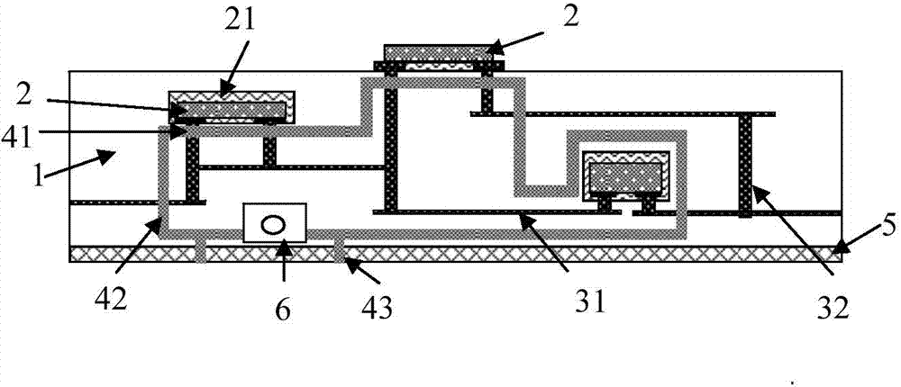
[0032] figure 1 and figure 2 They are respectively a three-dimensional schematic diagram and a cross-sectional view of an embodiment of the enhanced heat dissipation three-dimensional packaging structure of the present invention. Such as figure 1 and figure 2 As shown, the enhanced heat dissipation three-dimensional packaging structure of the present invention includes: a multilayer substrate 1, a device 2 on the substrate and an interconnection circuit 3 connecting the devices, a microchannel 4, a heat dissipation plate 5, an external heat dissipation device and a water pump 6; wherein, The microchannel 4 includes a horizontal groove 41 on each layer of the substrate and a corresponding via hole 42 in the vertical direction between each layer of the substrate to form an interconnected channel; the heat dissipation plate 5 is arranged on th...


PUM


Abstract

The invention discloses an enhanced radiation three-dimensional packaging structure and a packaging method for the same. The enhanced radiation three-dimensional packaging structure comprises a multilayer substrate, devices and an interconnection circuit for connecting the devices on the substrate, a micro-channel, a radiation plate, an external radiation device and a water pump. According to the enhanced radiation three-dimensional packaging structure and the packaging method for the same, a micro-fluid convection heat transfer mode is used for quickly conducting away the vast majority of heat produced by heating devices, and the three-dimensional interconnection circuit consisting of good metal conductors connected with the heating devices in the substrate is used for assisting the conduction of the heat into and out of the substrate in a metal heat conduction way; the radiation plate at the bottom of the substrate can be connected with various types of external radiation devices, so that the problem of thermally-induced failures of a multi-chip electronic product is effectively solved; process conditions are easy to implement, and the enhanced radiation three-dimensional packaging structure and the packaging method for the same are low in cost and convenient to machine in batches, and can be widely applied to a plurality of fields of aerospace, information communication, biochemistry, medicines, automatic control, consumer electronics and the like related to national electronic development and national security.

Description

technical field [0001] The invention relates to the heat dissipation technology of microelectronic devices, in particular to a three-dimensional packaging structure for enhanced heat dissipation of micro devices based on multilayer packaging substrate technology and a packaging method thereof. Background technique [0002] The information technology of society and the development of microelectronics technology make electronic devices show the development trend of miniaturization, high performance and multifunctionality, integrating multiple micro devices, microstructures, sensors, actuators, signal processing, control circuits, The MCM multi-chip module and microsystem technology of interface, communication and power supply have been developed rapidly, and its manufacturing processes such as chip processing, integrated assembly, packaging and testing are more complicated than those of planar integrated circuits. As the last step in the formation of microelectronic products, ...

Claims


Application Information

Patent Timeline
Patent Type & Authority Applications(China)
IPC IPC(8): H01L23/473H01L23/467
CPCH01L2224/16225H01L2924/1627
Inventor 张杨飞张兰英
Owner PEKING UNIV
Why Eureka
Try Eureka