Local aluminum back surface field solar battery with two diaphanous faces and preparation method thereof
A solar cell, aluminum back field technology, applied in photovoltaic power generation, circuits, electrical components, etc., can solve problems such as affecting photoelectric conversion efficiency, and achieve the effect of improving photoelectric conversion efficiency, reducing dosage, and promoting photoelectric performance.
- Summary
- Abstract
- Description
- Claims
- Application Information
AI Technical Summary
Problems solved by technology
Method used
Image
Examples
Embodiment 1
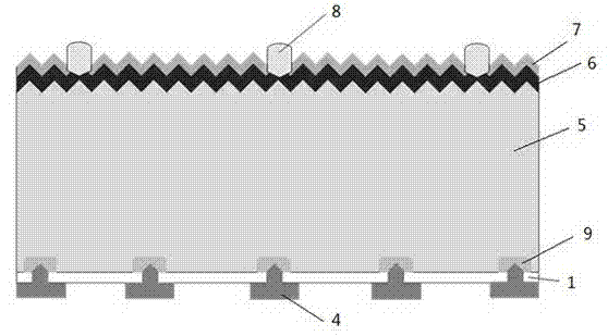
[0041] This example illustrates the structure and preparation method of a double-sided light-transmitting partial aluminum back field crystalline silicon solar cell (the cross-sectional view of the cell is shown in figure 1 ),Specific steps are as follows:
[0042] A. Select a lightly doped p-type single crystal silicon wafer with a resistivity of 0.1~10 Ω·cm, and place it in a velvet tank. , the surface texture is carried out at a temperature of 75-90°C to form a suede structure;
[0043] B. Clean the surface of the silicon wafer with a chemical solution. The chemical solution can be one or more mixed aqueous solutions of hydrofluoric acid, nitric acid, hydrochloric acid, sulfuric acid and other additives. The cleaning time can be 0.5 to 60 minutes. The temperature can be 5~90℃;
[0044] C. After cleaning the above textured sheet, place it in a furnace tube at 700~1000°C for phosphorus (P) diffusion to prepare an n-type emitter. The diffusion time can be 70~150 minutes, and...
Embodiment 2
[0058] This example illustrates a double-sided light-transmitting partial aluminum back field crystal silicon solar cell structure and its preparation method (see the attached figure 1 ),Specific steps are as follows:
[0059] A. Select a lightly doped p-type polysilicon wafer with a resistivity of 0.1~10 Ω cm, place it in a velvet tank, and place it in a 0.5~5% sodium hydroxide deionized aqueous solution by weight, Under the condition of temperature of 75~90℃, the surface texture is formed to form a suede structure;
[0060] B. Clean the surface of the silicon wafer with a chemical solution. The chemical solution is one or more mixed aqueous solutions of hydrofluoric acid, nitric acid, hydrochloric acid, sulfuric acid and other additives. The cleaning time is 0.5 to 60 minutes and the temperature is 5 ~90℃;
[0061] C. After cleaning the above textured sheet, place it in a furnace tube at 700~1000°C for phosphorus (P) diffusion to prepare an n-type emitter. The diffusion ti...
Embodiment 3
[0070] This example illustrates the structure and preparation method of a double-sided light-transmitting partial aluminum back field crystalline silicon solar cell (the cross-sectional view of the cell is shown in figure 1 ),Specific steps are as follows:
[0071] A. Select a lightly doped p-type single crystal silicon wafer with a resistivity of 0.1~10 Ω·cm, and place it in a velvet tank. , the surface texture is carried out at a temperature of 75-90°C to form a suede structure;
[0072] B. Clean the surface of the silicon wafer with a chemical solution. The chemical solution can be one or more mixed aqueous solutions of hydrofluoric acid, nitric acid, hydrochloric acid, sulfuric acid and other additives. The cleaning time can be 0.5 to 60 minutes. The temperature can be 5~90℃;
[0073] C. After cleaning the above textured sheet, place it in a furnace tube at 700~1000°C for phosphorus (P) diffusion to prepare an n-type emitter. The diffusion time can be 70~150 minutes, and...
PUM
| Property | Measurement | Unit |
|---|---|---|
| Width | aaaaa | aaaaa |
| Aperture | aaaaa | aaaaa |
| Hole spacing | aaaaa | aaaaa |
Abstract
Description
Claims
Application Information
 - R&D
- Intellectual Property
- Life Sciences
- Materials
- Tech Scout
- Unparalleled Data Quality
- Higher Quality Content
- 60% Fewer Hallucinations
Browse by: Latest US Patents, China's latest patents, Technical Efficacy Thesaurus, Application Domain, Technology Topic, Popular Technical Reports.
© 2025 PatSnap. All rights reserved.Legal|Privacy policy|Modern Slavery Act Transparency Statement|Sitemap|About US| Contact US: help@patsnap.com


