Preparation method of low surface pore and low dielectric constant thin-film material

A low-dielectric constant, thin-film material technology, applied in the manufacture of circuits, electrical components, semiconductors/solid-state devices, etc., to achieve the effects of small bombardment, good continuity, and reduced pores

Inactive Publication Date: 2014-01-22
SUZHOU UNIV
View PDF2 Cites 4 Cited by
  • Summary
  • Abstract
  • Description
  • Claims
  • Application Information

AI Technical Summary

Problems solved by technology

[0005] In view of this, the present invention provides a kind of preparation method of low surface porosity low dielectric constant film material, to overcome the deficiency of existing preparation method

Method used


Image

  • Preparation method of low surface pore and low dielectric constant thin-film material
  • Preparation method of low surface pore and low dielectric constant thin-film material
  • Preparation method of low surface pore and low dielectric constant thin-film material

Examples


preparation example Construction

[0031] A kind of preparation method of low surface porosity low dielectric constant film material of the present invention, it comprises the steps:

[0032] (1) Provide a silicon substrate, clean it, and place the cleaned silicon substrate in an electron cyclotron resonance plasma device. Preferably, the aforementioned silicon substrate is a (100)-oriented n-type silicon substrate. And the above cleaning method is standard cleaning.

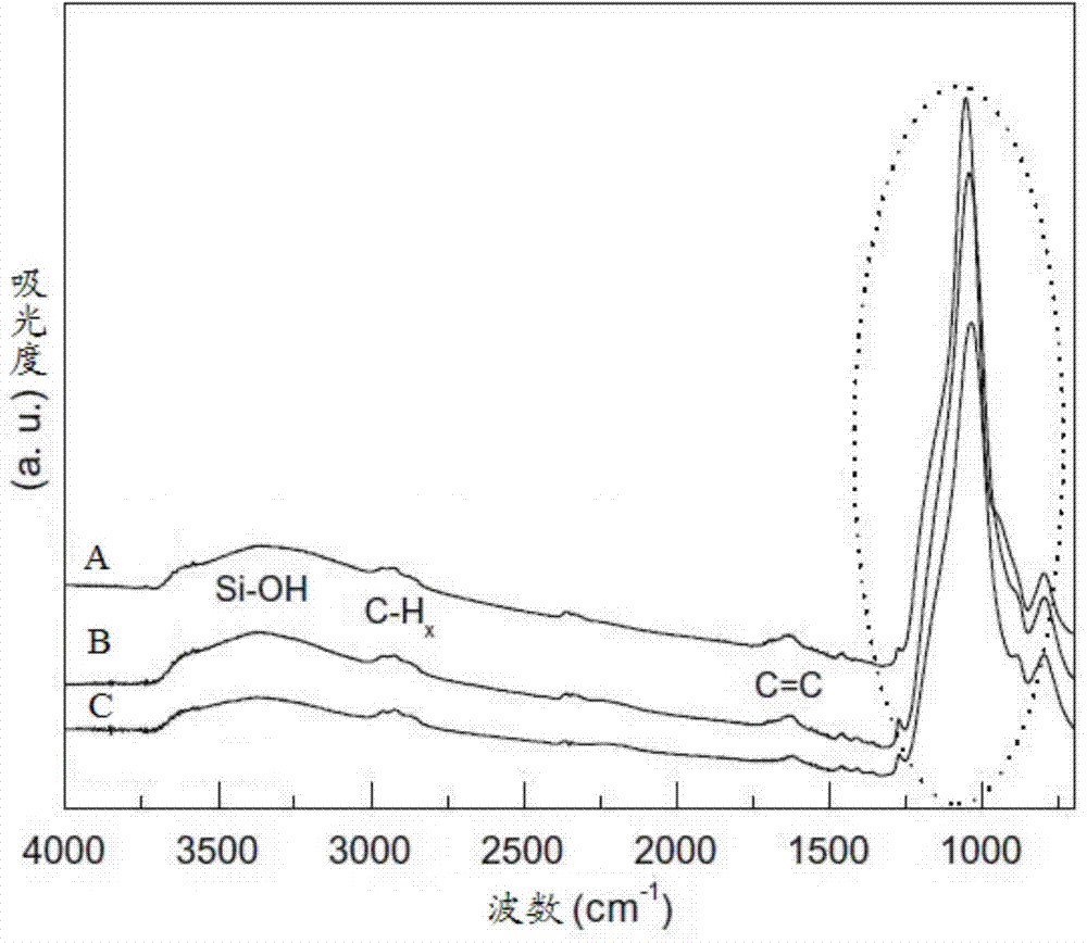
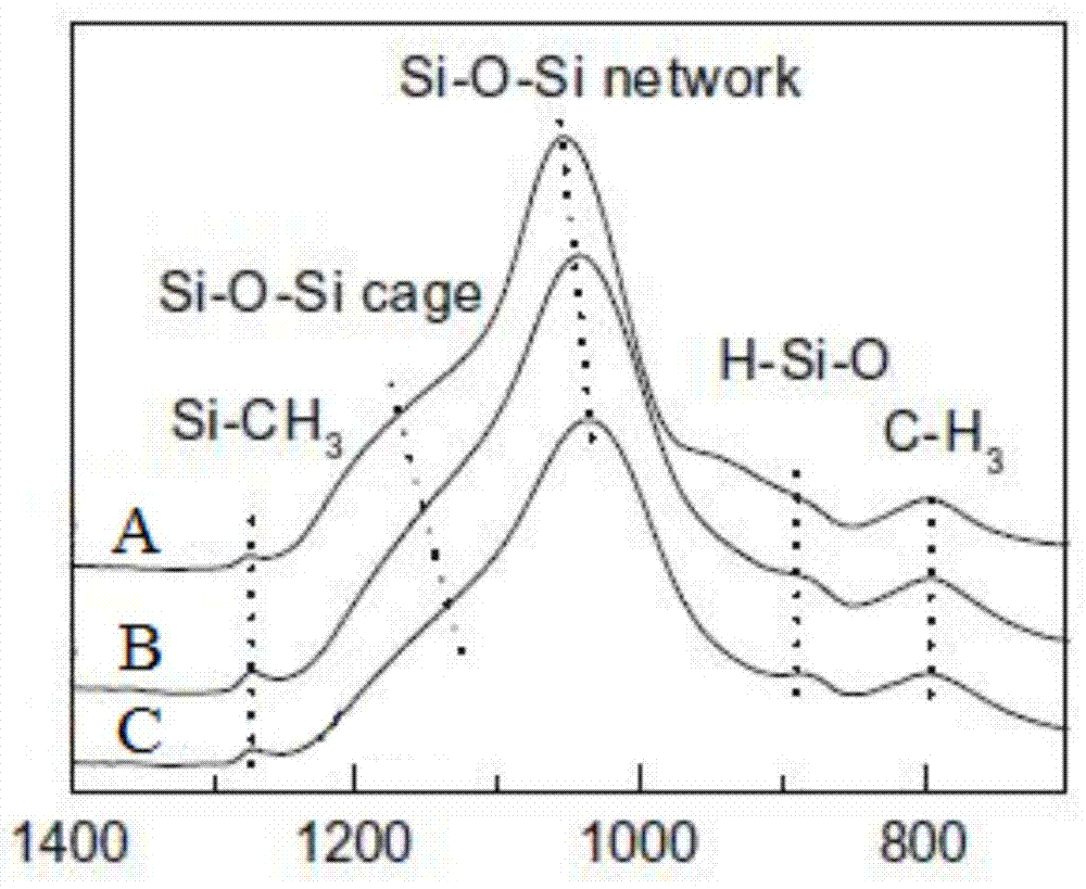
[0033] (2) Place the D5 ring silicone in a constant temperature evaporator, and use the inert gas as the carrier gas to transport the vaporized D5 ring silicone to the electron cyclotron resonance plasma device through the transmission pipeline. Among them, the D5 ring silicone is a single ring structure consisting of five Si-O bonds and ten methyl groups. The constant temperature in the above-mentioned constant temperature evaporator is preferably 80°C, and at the same time, in order to prevent the vaporized D5 ring silicone from being liquefi...

Embodiment 1

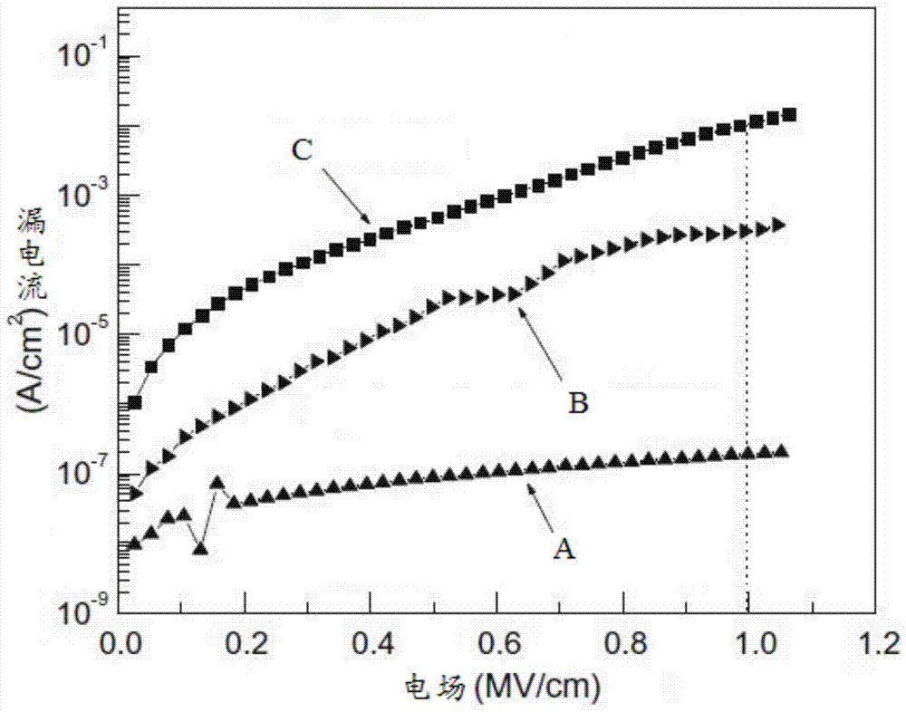
[0041] Provide a low-resistance single crystal silicon substrate, perform standard clearing on it, and place it in an electron cyclotron resonance plasma device. D5 ring silicone with a purity of 98% was prepared as a precursor, and the D5 ring silicone was placed in a constant temperature evaporator at 80 °C to vaporize it. Using argon as a carrier gas, the vaporized D5 ring organosilicon was sent into the cavity of the electron cyclotron resonance plasma equipment through a transmission pipeline at 80 °C, and the flow ratio of the vaporized D5 ring organosilicon and argon was kept at 6. :1, the total gas flow rate is controlled at 15 sccm. Controlling the current I of two coils in an electron cyclotron resonance plasma device 1 and I 2 They are 150A and 110A respectively, the microwave incident power is 300W, and the reflected power is 2%. The D5 ring organic silicon forms a plasma and decomposes, and deposits a SiCOH film on a silicon substrate under the action of a magn...

Embodiment 2

[0044] The difference between this embodiment and embodiment 1 is that the microwave incident power is controlled to be 800 W when oxygen is introduced, and the other steps are the same as those of embodiment 1, and will not be repeated here.


PUM

PropertyMeasurementUnit
thicknessaaaaaaaaaa
current densityaaaaaaaaaa

Abstract

The invention discloses a preparation method of a low surface pore and low dielectric constant thin-film material. The preparation method comprises steps as follows: a silicon substrate is provided, cleaned and placed in electron cyclotron resonance plasma equipment; decamethylcyclopentasiloxane is placed in a constant-temperature evaporator and sent into the electron cyclotron resonance plasma equipment; a controller is adjusted to enable decamethylcyclopentasiloxane to form a plasma, and a porous SiCOH thin film is formed on the surface of the silicon substrate through deposition; and the porous SiCOH thin film obtained through deposition is placed on a work station for hole sealing treatment of the surface of the plasma. According to the preparation method, the continuity of the preparation process is good, and the thin-film material is prevented from being exposed to the atmosphere and polluted; the low surface pore and low dielectric constant thin-film material prepared with the preparation method suffers smaller bombardment and is high in quality; and simultaneously, the surface pores of the material are reduced, the diffusion of copper in the surface of a low dielectric constant thin film is reduced, and the electrical property of a copper/low dielectric constant material integrated system is effectively improved.

Description

technical field [0001] The invention relates to the technical field of integrated circuits, in particular to a preparation method of a thin-film material with low surface porosity and low dielectric constant. Background technique [0002] With the improvement of the integration level of large-scale integrated circuits, the characteristic line width scale is reduced to tens of nanometers, and the RC delay of the internal connection layer becomes an important issue affecting the performance of the device, which will cause signal transmission delay, increase power consumption and metal internal connection Increased crosstalk between layers. In order to solve these problems, it is necessary to replace SiO with low dielectric constant material and low resistivity metal interconnection layer. 2 / Al structure. Low dielectric constant materials and ultra-low dielectric constant materials as SiO 2 Alternatives have attracted widespread attention. Among all the studied porous low...

Claims


Application Information

Patent Timeline
Patent Type & Authority Applications(China)
IPC IPC(8): H01L21/31
CPCH01L21/76826H01L21/3105H01L21/76898
Inventor 叶超廖良生袁大星王响英
Owner SUZHOU UNIV
Why Eureka
Try Eureka