Silicon nano wire quantum well solar cell and preparation method thereof

A technology of solar cells and silicon nanowires, applied in circuits, photovoltaic power generation, electrical components, etc., can solve the problems of insufficient utilization of photon energy, limited effective photoelectric conversion area, and low carrier collection efficiency, and achieve photoelectric High replacement efficiency, long service life and low cost

Inactive Publication Date: 2014-02-19
JIANGSU UNIV
View PDF5 Cites 5 Cited by
  • Summary
  • Abstract
  • Description
  • Claims
  • Application Information

AI Technical Summary

Problems solved by technology

[0005] Silicon nanowire / amorphous silicon heterojunction solar cell (CN101262024A) patent and a new structure silicon nanowire solar cell (CN101369610A) patent only use amorphous silicon materials with a single band gap to make solar cells, because the energy is smaller than this band gap The photons in the band gap cannot be absorbed, resulting in low energy loss, while the excess energy of the photons larger than this band gap is lost in the form of heat energy, resulting in the photon energy not being fully utilized
Nc - Si:H / SiN x The superlattice quantum well solar cell (CN102157594 A) patent adopts the traditional planar cell structure, which not only has a relatively high surface reflectance, but also has a limited effective photoelectric conversion area that can receive light, and a very long load between the upper and lower electrodes of the planar cell. Carrier transport distance leads to very low carrier collection efficiency

Method used


Image

  • Silicon nano wire quantum well solar cell and preparation method thereof
  • Silicon nano wire quantum well solar cell and preparation method thereof
  • Silicon nano wire quantum well solar cell and preparation method thereof

Examples


Embodiment Construction

[0028] The specific embodiments of the present invention will be further described below in conjunction with the accompanying drawings.

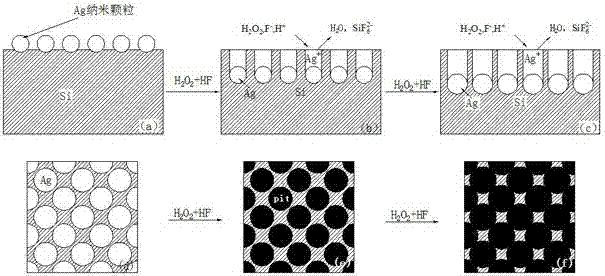
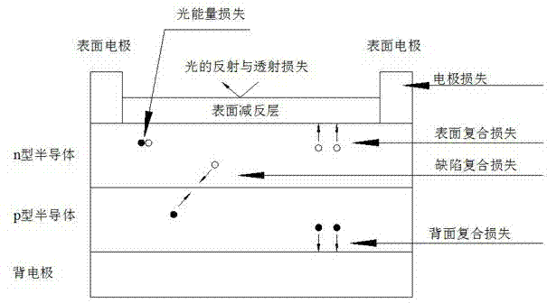
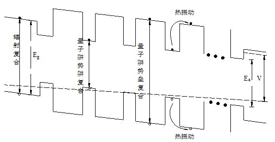
[0029] Such as Figure 5 As shown, Al / p + / p / nc-Si:H / SiN x Superlattice quantum well / n / n + A new type of solar cell with / AZO structure, the silicon nanowire quantum well solar cell is sequentially composed of Ti / Pd / Ag grid electrode, transparent aluminum-doped zinc oxide (AZO) conductive layer film, n+ ohmic contact layer, n layer along the incident direction of sunlight , nc-Si:H / SiN x Superlattice quantum wells, p-type silicon nanowire arrays, p + Ohmic contact layer and Al back electrode. The thickness of each monolayer of Nc-Si is controlled at 9±0.5 nm, and the period is 45±5 nm; SiN x The thickness of each monolayer is controlled at 9±0.5 nm, and the period is 45±5 nm.

[0030] Such as figure 2 As shown in the graph comparing the reflectivity of the silicon nanowire array and the reflectivity of the polished silicon wafer, t...


PUM


Abstract

The invention discloses a silicon nano wire quantum well solar cell. A Ti/Pd/Ag grid electrode, a transparent aluminum-doped zinc oxide (AZO) conductive layer film, an n<+> ohmic contact layer, an n layer, an nc-Si:H/SiNx superlattice quantum well, a p<+> ohmic contact layer and an AL back electrode are sequentially arranged along an incident sunshine direction, a solar cell employs a p-type silicon nano wire array to support the nc-Si:H/SiNx superlattice quantum well. The solar cell preparation method is further disclosed. The solar cell has advantages of high light tripping, high efficiency, low cost and long service life. A gradual change type quantum well material is formed at a surface of the silicon nano wire array, so a light tripping effect of the solar cell is greatly improved, a light absorption spectrum of the solar cell is further widened, and the approximate full-spectrum nc-Si:H/SiNx superlattice quantum well solar cell is formed.

Description

technical field [0001] The present invention relates to the field of new energy technologies such as nanotechnology and photovoltaic technology, and designs a method that uses silicon nanowires as a support to deposit nc-Si:H and SiN on silicon nanowires. x Novel silicon nanowire solar cells comprising superlattice quantum well materials. Background technique [0002] Traditional energy such as coal, oil, and natural gas will be exhausted. The environmental pollution they cause is very serious, such as water pollution, air pollution, dust pollution, etc., which seriously endanger people's health and living environment. Facing the global energy shortage crisis and the continuous deterioration of the ecological environment, countries all over the world are actively researching, developing and utilizing new energy sources. Renewable energy, especially solar energy, has attracted more and more attention. As an important way to utilize solar energy, photovoltaic applications ha...

Claims


Application Information

Patent Timeline
Patent Type & Authority Applications(China)
IPC IPC(8): H01L31/0352H01L31/06H01L31/18
CPCY02E10/50H01L31/028H01L31/035254H01L31/1804Y02E10/547Y02P70/50
Inventor 丁建宁张福庆郭立强袁宁一程广贵凌智勇张忠强
Owner JIANGSU UNIV
Why Eureka
Try Eureka