

Copper nanowire and preparation method thereof
A nano-copper wire, copper salt technology, applied in nanotechnology, nanotechnology, nanotechnology for materials and surface science, etc., can solve the problems of poor uniformity of nano-metal wires, damage to conductivity and structure, and high cost of synthesis methods , to achieve the effect of simple equipment, low cost, good dispersibility and oxidation resistance
- Summary
- Abstract
- Description
- Claims
- Application Information
AI Technical Summary
Problems solved by technology
Method used
Image

Examples
Embodiment 1
[0038] The preparation method of nano copper wire of the present embodiment comprises the following steps:
[0039] (1) Take 0.5L 1mol / L calcium hydroxide solution in the reactor, start the magnetic stirrer and ultrasonic generator, heat to 50°C, add 20μL 0.01mol / L copper acetate solution and stir evenly;
[0040] (2) Take 200mL of 0.005mol / L potassium borohydride solution and 1×10 -3 mol / L polyvinylpyrrolidone solution 25mL is mixed evenly, then added to the solution obtained in step (1) and stirred evenly;
[0041] (3) Add 1L of 0.01mol / L copper acetate solution at a rate of 2.0mL / min and keep reacting for 0.5 hours at a reaction temperature of 50°C;
[0042] (4) The product obtained in step (3) is centrifuged and washed with absolute ethanol and distilled water to obtain the nano copper wire.
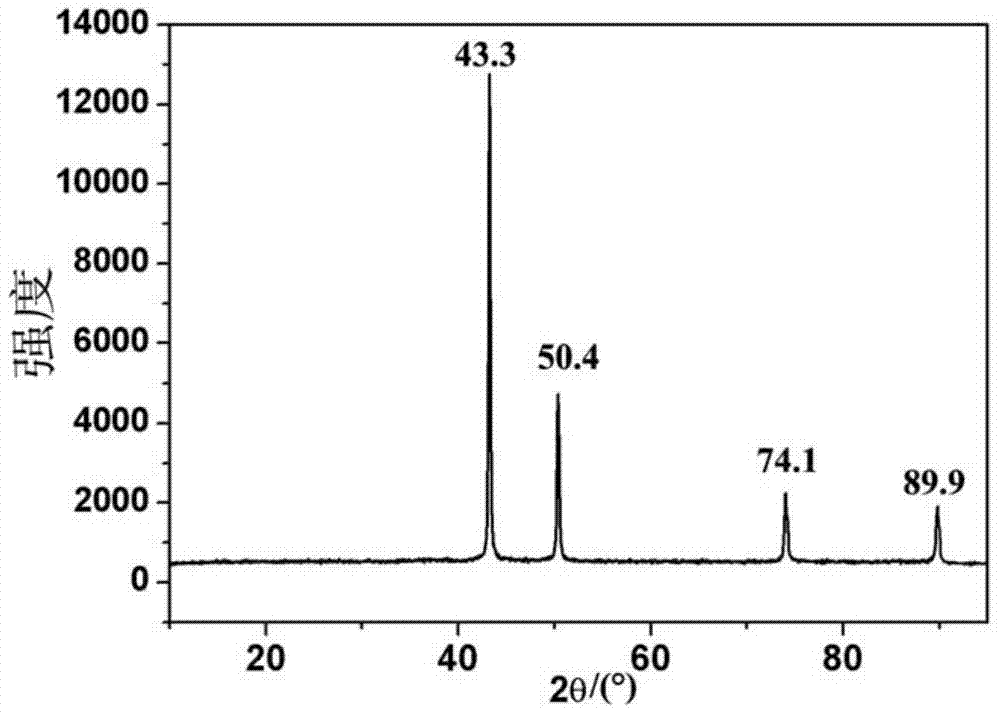
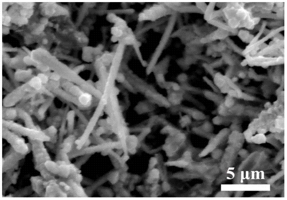
[0043] The above product was analyzed by X-ray diffraction (XRD, such as figure 1 shown) and EDS (as Figure 8 Shown) analysis is pure copper; SEM observes the morphology and str...
Embodiment 2
[0045] The preparation method of nano copper wire of the present embodiment comprises the following steps:
[0046] (1) Take 0.2L 5mol / L sodium hydroxide solution in the reactor, start the magnetic stirrer and ultrasonic generator, heat to 40°C, add 40μL 0.0005mol / L copper sulfate solution and stir evenly;
[0047] (2) Take 10mL of 0.005mol / L sodium borohydride solution and 1×10 -3 mol / LC 13 ~C16 Mix 20mL sodium alkyl sulfonate solution evenly, add it to the solution obtained in step (1), and stir evenly;
[0048] (3) Add 1L of 0.05mol / L copper sulfate solution at a rate of 0.4mL / min and keep reacting for 2 hours at a reaction temperature of 40°C;
[0049] (4) Centrifuge the reaction product obtained in step (3), wash it with absolute ethanol and distilled water to obtain the copper nanowire of this embodiment.
[0050] The X-ray diffraction analysis (XRD) figure is similar to that of Example 1; the morphology and structure of the nano-copper wires obtained in this example ...
Embodiment 3
[0052] The preparation method of nano copper wire of the present embodiment comprises the following steps:
[0053] (1) Take 0.1L 8mol / L potassium hydroxide solution in the reactor, start the magnetic stirrer and ultrasonic device, and heat to 70°C, add 60μL 0.01mol / L copper nitrate solution and stir evenly;
[0054] (2) Take 300mL of 0.015mol / L glucose solution and 1×10 -4 mol / L sodium lauryl sulfate 15mL is mixed evenly, then added to the solution obtained in step (1), and stirred evenly;
[0055] (3) Add 1L of 0.01mol / L copper nitrate solution at a rate of 1.2mL / min and keep reacting for 3 hours at a reaction temperature of 70°C;
[0056] (4) Centrifuge the product obtained in step (3), wash it with absolute ethanol and distilled water to obtain the nano copper wire of this example.
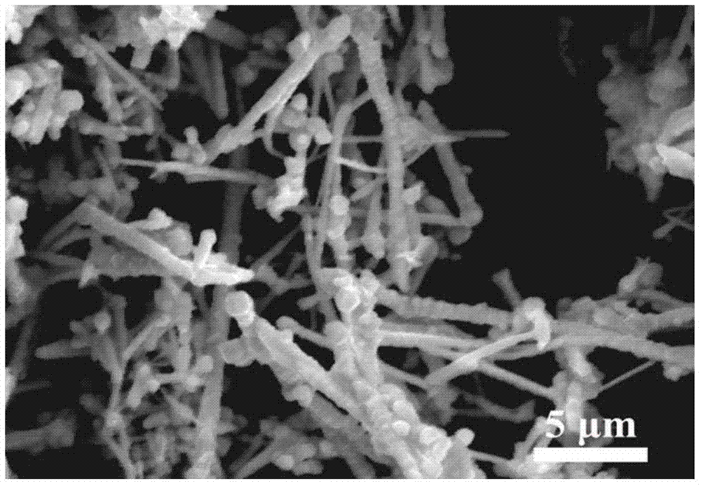
[0057] The X-ray diffraction analysis (XRD) figure is similar to that of Example 1; the morphology and structure of the nano-copper wires obtained in this example are observed by SEM, as F...
PUM
| Property | Measurement | Unit |
|---|---|---|
| diameter | aaaaa | aaaaa |
| diameter | aaaaa | aaaaa |
| length | aaaaa | aaaaa |
Abstract
Description
Claims
Application Information