Organic light-emitting device and preparation method thereof
An electroluminescent device and luminescence technology, which is applied in the direction of electric solid-state devices, semiconductor/solid-state device manufacturing, electrical components, etc., can solve the problems of easy luminescence quenching of light-emitting devices, thin electron injection layer thickness, and difficult process control. Achieve the effects of reducing the probability of luminescence quenching, reducing potential barriers, and improving luminescence performance
- Summary
- Abstract
- Description
- Claims
- Application Information
AI Technical Summary
Problems solved by technology
Method used
Image

Examples
Embodiment 1
[0073] A method for preparing an organic electroluminescent device, comprising the following steps:
[0074] (1) Conductive anode substrate pretreatment
[0075] Clean the ITO substrate with a thickness of 100nm with detergent, deionized water, acetone, and ethanol in sequence, for 5 minutes each time, then stop for 5 minutes, and repeat 3 times respectively; then dry it in an oven for use; Thereafter, it was treated with oxygen plasma for 10 minutes at a power of 35W.
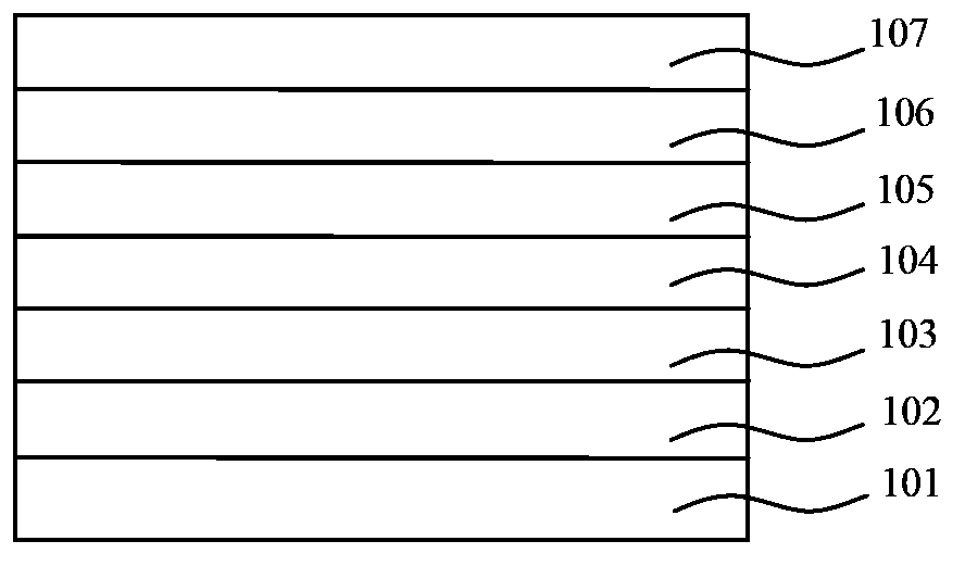
[0076] (2) Preparation of hole injection layer, hole transport layer, red light emitting layer, electron transport layer, electron injection layer
[0077] Place the pretreated ITO substrate in a vacuum chamber and evacuate to 1×10 -5 Pa, then MoO 3Incorporate N,N'-diphenyl-N,N'-di(1-naphthyl)-1,1'-biphenyl-4,4'-diamine (NPB) according to the doping concentration of 30wt% as hole injection layer to A hole injection layer with a thickness of 12.5nm is evaporated on the ITO substrate at an evaporation spee...
Embodiment 2
[0086] A method for preparing an organic electroluminescent device, comprising the following steps:
[0087] (1) Conductive anode substrate pretreatment
[0088] The FTO substrate with a thickness of 100nm was ultrasonically cleaned with detergent, deionized water, acetone, and ethanol in sequence. Each time, it was cleaned for 5 minutes, and then stopped for 5 minutes. Repeated 3 times respectively; and then dried in an oven for use; Thereafter, it was treated with oxygen plasma for 10 minutes at a power of 35W.
[0089] (2) Preparation of hole injection layer, hole transport layer, red light emitting layer, electron transport layer, electron injection layer
[0090] Place the pretreated FTO substrate in a vacuum chamber and evacuate to 5×10 -5 Pa, then WO 3 Doped into 4,4',4"-tris(carbazol-9-yl)triphenylamine (TCTA) as a hole injection layer according to the doping concentration of 25wt%, to A hole injection layer with a thickness of 10nm is evaporated on the FTO substr...
Embodiment 3
[0099] A method for preparing an organic electroluminescent device, comprising the following steps:
[0100] (1) Conductive anode substrate pretreatment
[0101] The AZO substrate with a thickness of 100nm was ultrasonically cleaned with detergent, deionized water, acetone, and ethanol in sequence. Each time, it was cleaned for 5 minutes, and then stopped for 5 minutes. Repeated 3 times respectively; and then dried in an oven for use; Thereafter, it was treated with oxygen plasma for 10 minutes at a power of 35W.
[0102] (2) Preparation of hole injection layer, hole transport layer, red light emitting layer, electron transport layer, electron injection layer
[0103] Place the pretreated AZO substrate in a vacuum chamber and evacuate to 5×10 -5 Pa, then V 2 o 5 Doped into 4,4'-bis(9-carbazole)biphenyl (CBP) as a hole injection layer according to the doping concentration of 35wt%, to A hole injection layer with a thickness of 15nm is evaporated on the AZO substrate at an...
PUM
| Property | Measurement | Unit |
|---|---|---|
| Thickness | aaaaa | aaaaa |
| Thickness | aaaaa | aaaaa |
| Thickness | aaaaa | aaaaa |
Abstract
Description
Claims
Application Information
 - R&D
- Intellectual Property
- Life Sciences
- Materials
- Tech Scout
- Unparalleled Data Quality
- Higher Quality Content
- 60% Fewer Hallucinations
Browse by: Latest US Patents, China's latest patents, Technical Efficacy Thesaurus, Application Domain, Technology Topic, Popular Technical Reports.
© 2025 PatSnap. All rights reserved.Legal|Privacy policy|Modern Slavery Act Transparency Statement|Sitemap|About US| Contact US: help@patsnap.com