Method for adhesive magnetron sputtering thick film

A magnetron sputtering and thick film technology, which is applied in sputtering plating, processes for producing decorative surface effects, decorative arts, etc., can solve the problems of serious environmental pollution by electroplating method and poor quality of thermal evaporation deposited films, etc. Achieve the effect of avoiding environmental pollution problems, solving poor quality and wide process window

Active Publication Date: 2014-04-09
STATE GRID CORP OF CHINA +1
View PDF7 Cites 7 Cited by
  • Summary
  • Abstract
  • Description
  • Claims
  • Application Information

AI Technical Summary

Problems solved by technology

[0004] Aiming at the deficiencies of the prior art, the purpose of the present invention is to provide a method of magnetron sputtering thick film with glue, to solve the problems of serious environmental

Method used


Image

  • Method for adhesive magnetron sputtering thick film
  • Method for adhesive magnetron sputtering thick film
  • Method for adhesive magnetron sputtering thick film

Examples


Example Embodiment

[0032] Embodiment one

[0033] 1) Clean the substrate (SiC material):

[0034] The SiC material 1 to be etched is sequentially subjected to the following cleaning steps:

[0035] Organic contamination removal: 1# cleaning solution (ammonia: hydrogen peroxide: pure water = 1:1:5), temperature 70° for 5 minutes; inorganic contamination removal 2# cleaning solution (hydrochloric acid: hydrogen peroxide: pure water = 1:1 :5), temperature 70°, time 5 minutes; BOE cleaning solution (hydrofluoric acid: ammonium fluoride = 1:20), room temperature, time 30 seconds; acetone ultrasonication 5 minutes; isopropanol ultrasonication 5 minutes; DI water rinse 5 minutes Divide, dry, and set aside.

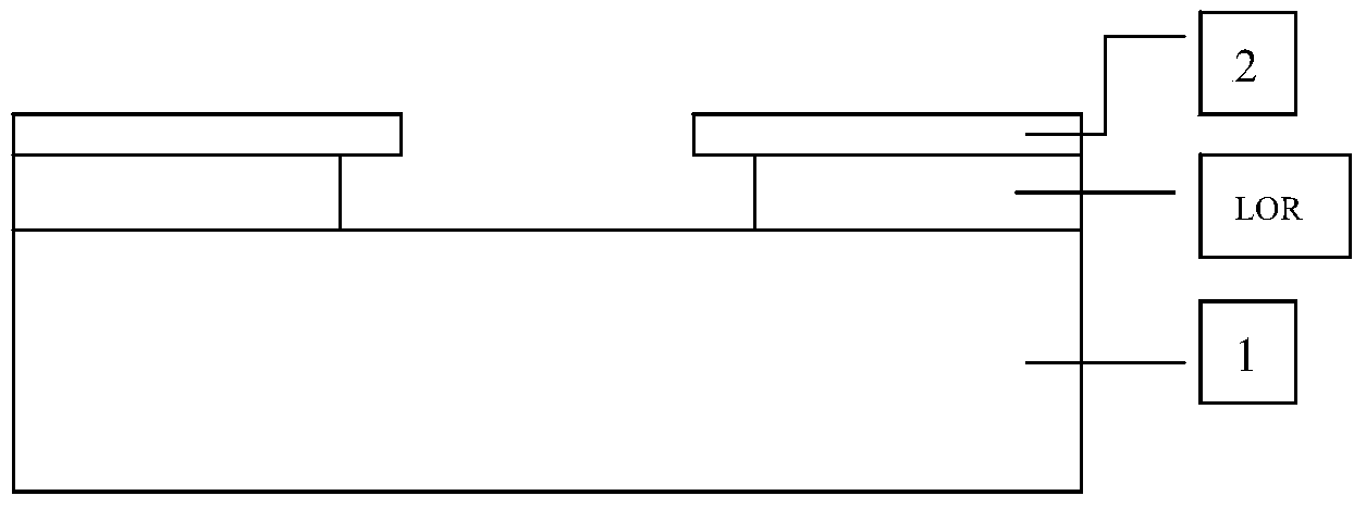
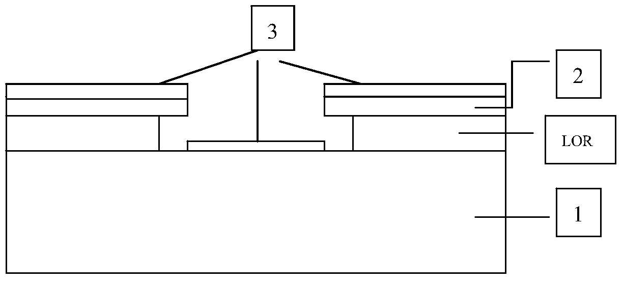
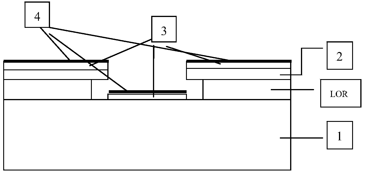
[0036] 2) Substrate photolithography, the process flow is as follows:

[0037] Glue coating: Vapor-phase coating of tackifier; spin-coating of LOR20B type peeling glue, the speed is 3000 rpm, the thickness is about 2um, and the baking time is 120s at 170°. Spin-coat photoresist 2, the glue type...

Example Embodiment

[0048] Embodiment two

[0049] 1) Clean the substrate (glass):

[0050] The SiC material 1 to be etched is sequentially subjected to the following cleaning steps:

[0051] Sonicate for 5 minutes in acetone; 5 minutes in isopropanol; rinse with DI water for 5 minutes, dry and set aside.

[0052] 2) Substrate photolithography, the process flow is as follows:

[0053] Coating: Vapor-phase coating of tackifier; spin-coating photoresist 2, glue type 4620, thickness 7um; pre-baking at 100 degrees Celsius for 180 seconds; SUSS MA6 photolithography machine contact exposure for 18 seconds; post-baking at 95 degrees Celsius for 20 seconds; 3038 The developing solution is developed for 45s; 110°, the time is 120s to harden the film, such as Image 6 shown.

[0054] 3) Substrate primer: M4L plasma glue remover primer, the process parameters are as follows:

[0055] Oxygen O2 flow rate 150sccm, RF power 200W, gluing time 2 minutes, base film inspection.

[0056] 4) High-power fast magn...


PUM


Abstract

The invention relates to a device manufacturing process, in particular to a method for an adhesive magnetron sputtering thick film. The method comprises the steps of sequentially conducting substrate cleaning, substrate photoetching, substrate bottom-adhesive coating, periodic thick-film deposition and peeling, wherein according to periodic thick-film deposition, high-power high-speed thin-film magnetron sputtering and low-power low-speed thin-film deposition are conducted in a period, and when periodic thick-film deposition is conducted, a substrate of the adhesive magnetron sputtering thick film is obtained by alternately controlling the magnetron sputtering power. The method changes the process that only the same power is adopted for magnetron sputtering of a thick film in the past, and therefore effectively solves the problem that a photoresist is carbonized or deforms because of being heated, and the method can be used for conveniently obtaining the substrate of the high-quality adhesive magnetron sputtering thick film at high speed. The method solves the problems that an electroplating method causes serious pollution to the environment and thermal evaporation deposition thin films are poor in quality, achieves the technology of a wide process window, and is convenient and rapid to implement, economical and reliable.

Description

technical field [0001] The invention relates to a device manufacturing process, in particular to a method for magnetron sputtering a thick film with glue. Background technique [0002] Magnetron sputtering is not only a method of semiconductor thin film deposition, but also a very important means of metal electrode preparation in the semiconductor device preparation process. [0003] In the preparation of SiC high-voltage devices, the electrodes of SiC devices must be thickened before packaging to improve the electrical contact reliability of the device, and at the same time improve the thermal conductivity of the device. The stripping process is often used to transfer the thickened electrode pattern, so Adhesives are required to deposit thick metal film layers. Conventional electrode thickening processes include thermal evaporation or electroplating. On the one hand, this electrochemical method needs to use a lot of chemical liquid, which is more serious to environmental p...

Claims


Application Information

Patent Timeline
IPC IPC(8): H01L21/203B81C1/00C23C14/35
CPCB81C1/00349C23C14/35H01L21/02529H01L21/02658
Inventor 陆敏田亮张昭杨霏
Owner STATE GRID CORP OF CHINA
Why Eureka
Try Eureka