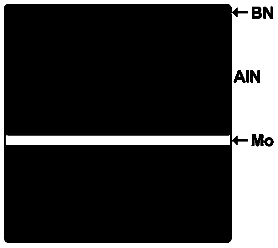
Method for preparing Mo/AlN/BN coating on surface of diamond/copper composite matrix
A diamond and substrate technology, applied in the direction of metal material coating process, coating, metal layered products, etc., can solve the problem of easy formation of oxide layer, etc., achieve good bonding, enhance film-base bonding strength, and low relative dielectric The effect of the coefficient
- Summary
- Abstract
- Description
- Claims
- Application Information
AI Technical Summary
Problems solved by technology
Method used
Image
Examples
Embodiment 1
[0025] 1. Substrate pretreatment
[0026] (1) Solvent cleaning treatment. First use isopropanol to ultrasonically clean for 15 minutes, then use 95% alcohol to ultrasonically clean for 15 minutes, and then rinse with ultrapure water for 3 minutes after taking it out.
[0027] (2) Ion source bombardment cleaning treatment. The substrate was cleaned by Hall ion source for 8 min, and the ambient pressure was 2.7×10 -2 Pa, Ar flow rate is 20sccm, substrate bias voltage is -150V, cathode current is 35A, cathode voltage is 25V, anode current is 7.8A, anode voltage is 95V.
[0028] 2. Deposit the metal Mo transition layer on the surface of the diamond / copper composite substrate by magnetron sputtering
[0029] (1) Mo metal target pretreatment. Heat the ambient temperature of the chamber to 175°C, use a mechanical pump and a molecular pump secondary device to evacuate the background of the deposition chamber, when the chamber pressure is ≤5.0×10 -5 After Pa, Ar was introduced, th...
Embodiment 2
[0043] 1. Substrate pretreatment
[0044] (1) Solvent cleaning treatment. With embodiment 1.
[0045] (2) Ion source bombardment cleaning treatment. With embodiment 1.
[0046] 2. Deposit the metal Mo transition layer on the surface of the diamond / copper composite substrate by magnetron sputtering
[0047] (1) Metal target pre-sputtering. With embodiment 1.
[0048] (2) Deposit a metal transition layer. With embodiment 1.
[0049] 3. Reactive sputtering deposition of AlN thin films
[0050] (1) Al target pre-sputtering. With embodiment 1.
[0051] (2) Deposit AlN film. will deposit N during 2 Flow is changed into 30%, and other steps are with embodiment 1.
[0052] 4. Deposit BN anti-oxidation protective layer on AlN film
[0053] (1) BN target pre-sputtering. With embodiment 1.
[0054] (2) Deposit BN anti-oxidation protective layer. With embodiment 1.
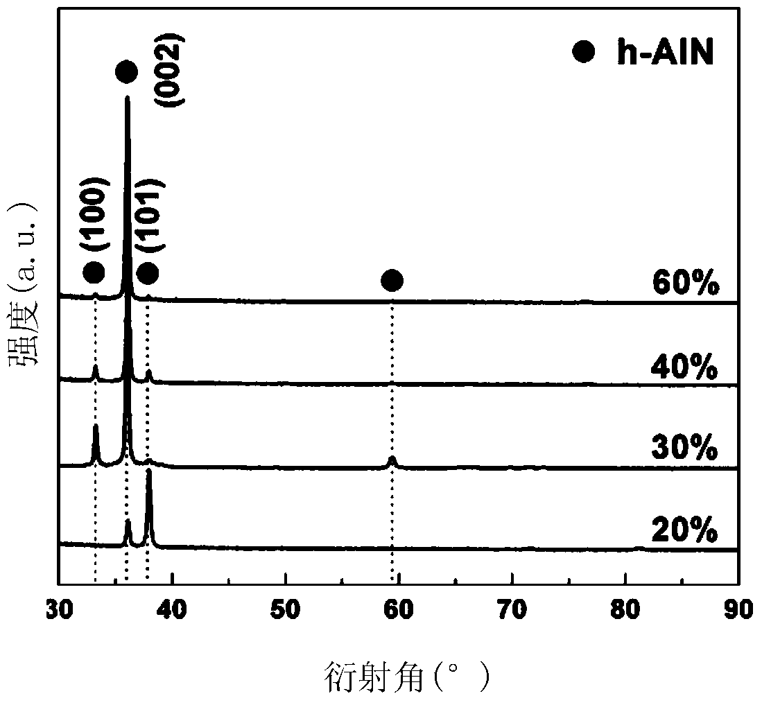
[0055] 5. Characterize 30%N by X-ray diffraction (XRD) 2 - Phase structure of Mo / AlN / BN coatings. figur...
Embodiment 3
[0061] 1. Substrate pretreatment
[0062] (1) Solvent cleaning treatment. With embodiment 1.
[0063] (2) Ion source bombardment cleaning treatment. With embodiment 1.
[0064] 2. Deposit the metal Mo transition layer on the surface of the diamond / copper composite substrate by magnetron sputtering
[0065] (1) Metal target pre-sputtering. With embodiment 1.
[0066] (2) Deposit a metal transition layer. With embodiment 1.
[0067] 3. Reactive sputtering deposition of AlN thin films
[0068] (1) Al target pre-sputtering. With embodiment 1.
[0069] (2) Deposit AlN film. will deposit N during 2 Flow is changed into 40%, and other steps are with embodiment 1.
[0070] 4. Deposit BN anti-oxidation protective layer on AlN film
[0071] (1) BN target pre-sputtering. With embodiment 1.
[0072] (2) Deposit BN anti-oxidation protective layer. With embodiment 1.
[0073] 5. Using X-ray diffraction (XRD) to characterize 40%N 2 - Phase structure of Mo / AlN / BN coatings. ...
PUM
| Property | Measurement | Unit |
|---|---|---|
| electrical resistivity | aaaaa | aaaaa |
| thickness | aaaaa | aaaaa |
| thickness | aaaaa | aaaaa |
Abstract
Description
Claims
Application Information


