Preparation method of trench gate in trench MOS device

A technology of MOS devices and trench gates, which is applied in semiconductor/solid-state device manufacturing, semiconductor devices, electrical components, etc., can solve the problems of easy concentration of electric field and affect the switching speed of trench-type MOS devices, etc., so as to reduce parasitic capacitance and reduce Switching loss, the effect of solving electrical breakdown

Inactive Publication Date: 2014-05-28
SHANGHAI HUAHONG GRACE SEMICON MFG CORP
View PDF6 Cites 13 Cited by
  • Summary
  • Abstract
  • Description
  • Claims
  • Application Information

AI Technical Summary

Problems solved by technology

In the above method, the thickness of the gate oxide film at the bottom of the trench is basically the same as the thickness of the gate oxide film on the sidewall of the trench, so the parasitic capacitance between the gate and the drain is large, which affects the switching speed o

Method used


Image

  • Preparation method of trench gate in trench MOS device
  • Preparation method of trench gate in trench MOS device
  • Preparation method of trench gate in trench MOS device

Examples


Embodiment Construction

[0027] The present invention will be described in further detail below in conjunction with the accompanying drawings and embodiments.

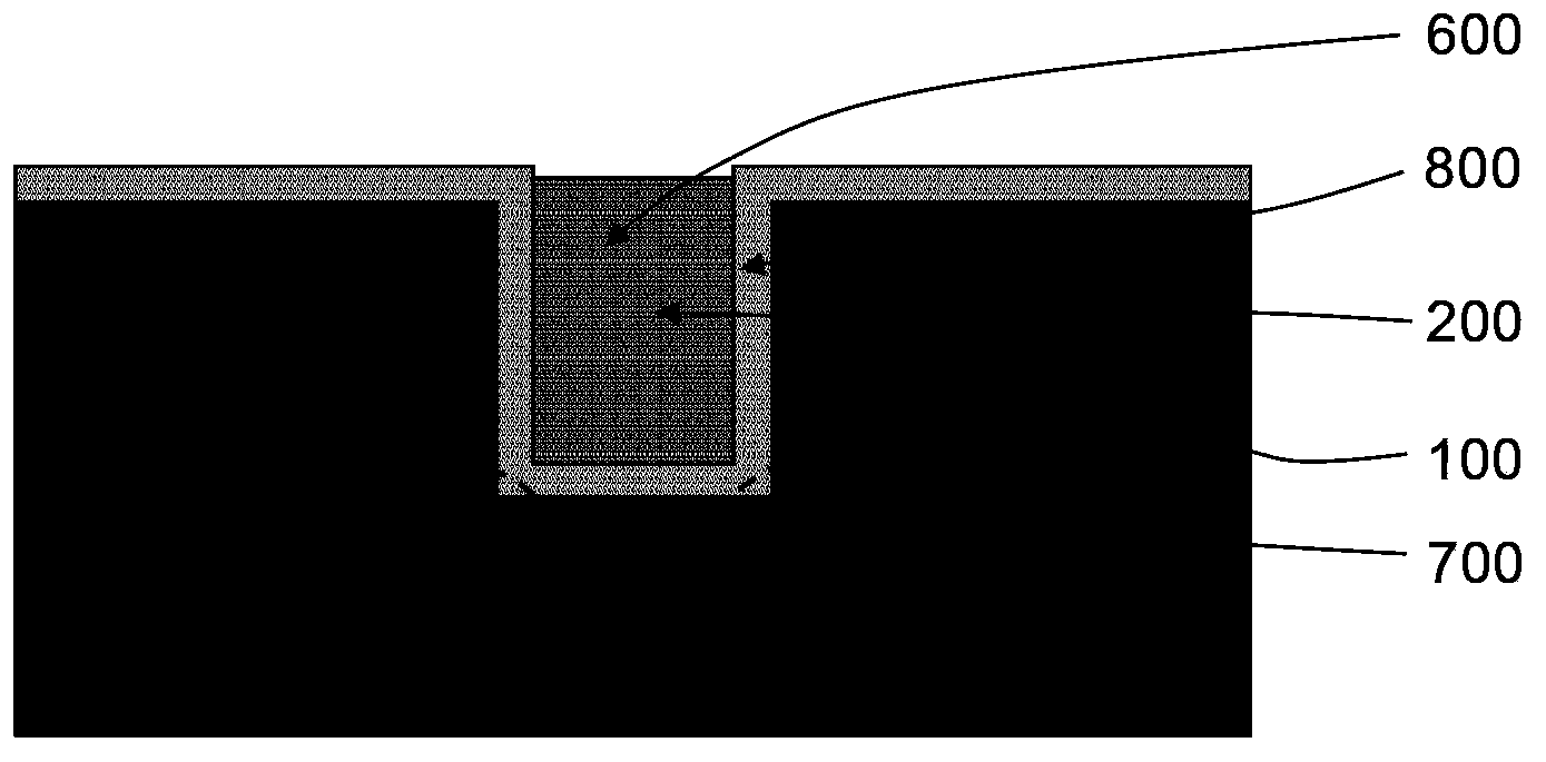
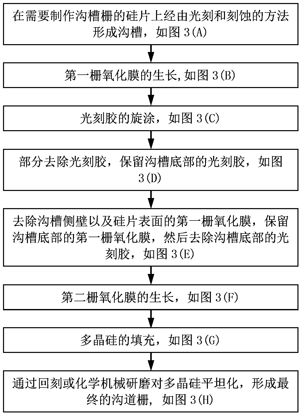
[0028] Such as figure 2 As shown in Fig. 3, the preparation method of trench gate in a kind of trench type MOS device of the present invention is characterized in that the gate oxide film at the bottom of the trench is thicker than the gate oxide film at the trench sidewall, comprising the following steps:

[0029] (1) As shown in Fig. 3 (A), on the silicon chip 100 that needs to make trench gate, form groove 200 through the method for photolithography and etching: described groove 200 is with photoresist pattern (in the figure not shown) is formed by etching a silicon wafer with a mask, or etching a silicon wafer with a dielectric film pattern (not shown in the figure) as a mask. Preferably, this embodiment uses a photoresist pattern as a mask, After dry etching the base silicon of the silicon wafer 100 and removing the photoresist, a trenc...


PUM

PropertyMeasurementUnit
Thicknessaaaaaaaaaa
Thicknessaaaaaaaaaa

Abstract

The invention discloses a preparation method of a trench gate in a trench MOS device. The preparation method of the trench gate in the trench MOS device is characterized in that the thickness of a gate oxidation film at the bottom of a trench is larger than the thickness of a gate oxidation film at the sidewall of the trench. The preparation method includes the following steps that: 1, a trench is formed on a silicon wafer through photo-etching and etching, and a trench gate is required to be produced on the silicon wafer; 2, a first gate oxidation film is grown; 3, spin coating of photoresist is performed; 4, the photoresist is removed partially, and part of the photoresist, which is located at the bottom of the trench, is reserved; 5, a part of the first gate oxidation film, which is located at the sidewall of the trench and the surface of the silicon wafer, is removed, and a part of the first gate oxidation film, which is located at the bottom of the trench, is reserved, and part of the photoresist, which is located at the bottom of the trench, is removed; 6, a second gate oxidation film is grown; polycrystalline silicon is filled; 8, planarization is performed on the polycrystalline silicon through etch-back or chemical mechanical lapping, and the final trench gate can be formed. With the preparation method of the trench gate in the trench MOS device of the invention adopted, parasitic capacitance between a gate and a drain can be reduced, and the switching speed of the trench MOS device can be improved, and switching loss can be decreased, and at the same time, the problem of proneness to electric breakdown at the bottom of the trench of the trench MOS device can be solved.

Description

technical field [0001] The invention relates to a semiconductor integrated circuit manufacturing process, in particular to a method for preparing a trench gate in a trench MOS device. Background technique [0002] In traditional planar MOS (Metal Oxide Semiconductor) devices, the source, gate and drain of the MOS transistors are all located on the horizontal plane of the silicon wafer, which not only occupies a large area, but also has a large on-resistance and power consumption. , unable to meet the requirements of miniaturization and low power consumption of power devices. The trench MOS device cleverly forms the gate of the transistor in a groove perpendicular to the surface of the silicon wafer, so that the conduction channel is transferred to the longitudinal direction of the silicon wafer. This has three advantages: (1) Reduce the device area , to further increase the device integration density, (2) effectively reduce the on-resistance and power consumption, (3) basic...

Claims


Application Information

Patent Timeline
IPC IPC(8): H01L21/28
CPCH01L21/28211H01L29/4236H01L29/42368
Inventor 郭晓波
Owner SHANGHAI HUAHONG GRACE SEMICON MFG CORP
Why Eureka
Try Eureka