Manufacturing method for SiC-based MOS device gate dielectric thin film

A technology of MOS devices and gate dielectrics, applied in semiconductor/solid-state device manufacturing, semiconductor devices, electrical components, etc., can solve the problems of low carrier mobility, high dielectric constant, low interface state density, etc., and achieve cost reduction , the effect of improving the preparation efficiency

Active Publication Date: 2014-06-25
厦门肖克利能源技术有限公司
View PDF6 Cites 15 Cited by
  • Summary
  • Abstract
  • Description
  • Claims
  • Application Information

AI Technical Summary

Problems solved by technology

[0004] The object of the present invention is to provide a method for preparing a gate dielectric film for SiC-based MOS devices, which is aimed at the low dielectric constant, high interface state density and low carrier mobility of the current SiC-based MOS device gate dielectric layer etc., to provide a gate dielectric film mainly used for MOS devices with high dielectric constant, high critical electric field and low interface state density with SiC and its preparation method

Method used


Image

  • Manufacturing method for SiC-based MOS device gate dielectric thin film
  • Manufacturing method for SiC-based MOS device gate dielectric thin film

Examples


Embodiment 1

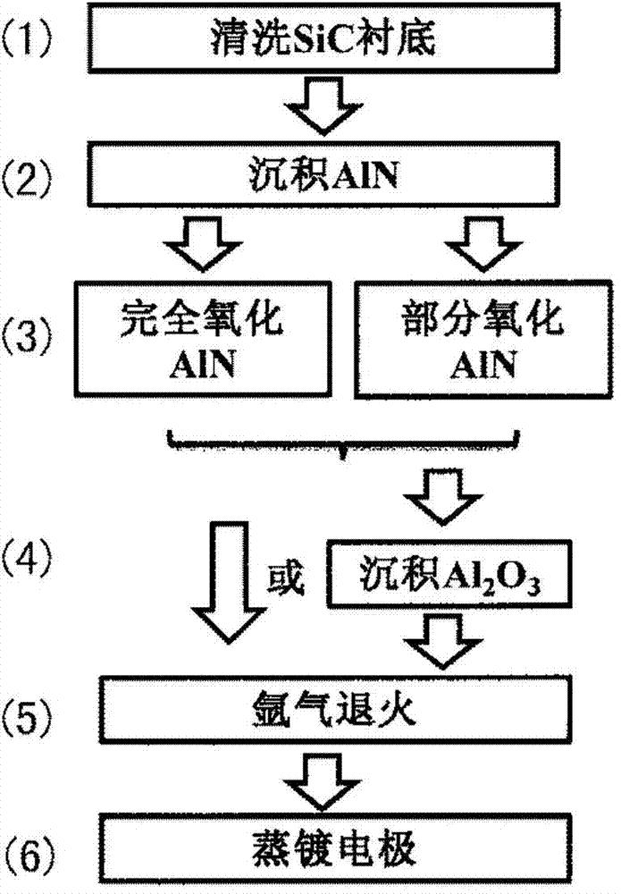
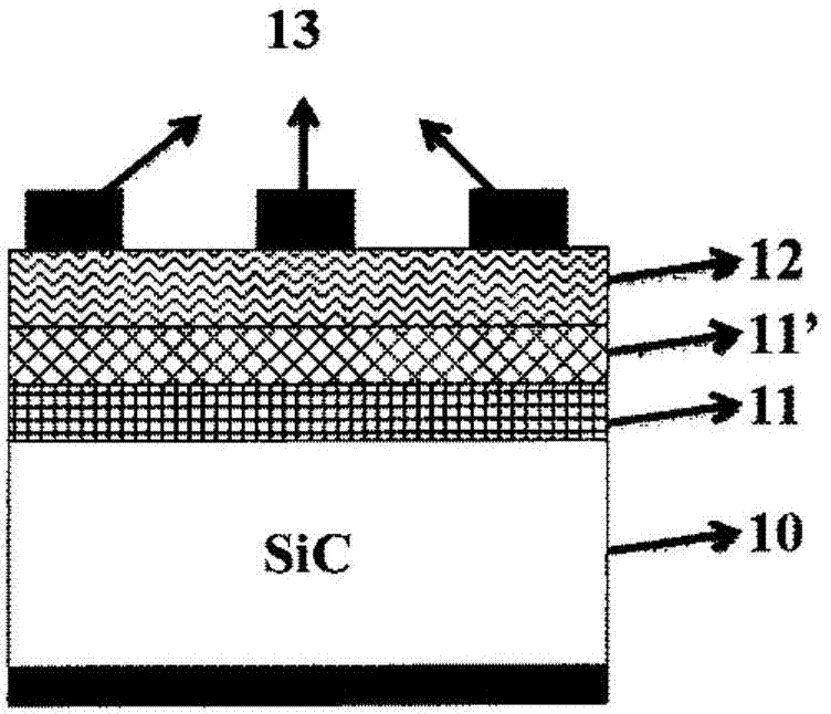
[0020] refer to figure 1 and refer to figure 2 , the invention provides a method for preparing a gate dielectric film for SiC-based MOS devices, comprising the following steps:

[0021] (1) Carry out standard cleaning to SiC substrate 10 samples:

[0022] a. Ultrasonic cleaning with toluene, acetone and ethanol three times in sequence, and then rinse with deionized water.

[0023] b. Soak the rinsed substrate in diluted hydrofluoric acid (hydrogen fluoride: deionized water = 1:3 by volume) for 1 min.

[0024] c. Boil the substrate soaked in hydrofluoric acid in concentrated sulfuric acid for 10 minutes.

[0025] d. Boil the substrate boiled in concentrated sulfuric acid with No. 1 solution and No. 2 solution for 1Smin, then rinse it with deionized water and dry it with nitrogen gas for later use. The No. 1 solution is ammonia water, hydrogen peroxide and deionized water The mixed solution of ammonia water: hydrogen peroxide: deionized water = 1:2:5 by volume, the No. 2 li...

Embodiment 2

[0032] refer to figure 1 and refer to figure 2 , the invention provides a method for preparing a gate dielectric film for SiC-based MOS devices, comprising the following steps:

[0033] Wherein step (1) and (2) are with embodiment 1;

[0034] Step (3) oxidize the AlN thin film 11 to Al by an oxidation method x o y Nz Thin film 11', where x, y, and z are stoichiometric ratios, controlled by the oxidation rate and oxidation time, the AlN film 11 is completely oxidized to Al x o y N z Thin film 11', which is a more stable film than AlN film 11, can play a role in reducing the interface state; the oxidation temperature is 1200°C;

[0035] Step (4) utilize atomic layer deposition to 10nm Al 2 o 3 Thin film 12 is deposited onto Al x o y N z On the film 11', the passivation performance of the Al2O3 film 12 is better, and the dielectric constant is the same as that of the AlN film 11 and Al x o y N z The thin film 11' is close to and can function as a passivation layer....


PUM


Abstract

A manufacturing method for an SiC-based MOS device gate dielectric thin film comprises the steps that an SiC substrate is cleaned; an AlN thin film is deposited on the cleaned SiC substrate; the AlN thin film is oxidized into an AlxOyNz thin film, through oxidization technology control, the AlN thin film is oxidized into the AlxOyNz thin film completely or partially, and an AlN/AlxOyNz gate dielectric layer is formed; an Al2O3 thin film is deposited onto the AlxOyNz thin film to form an AlxOyNz/Al2O3 stacked gate dielectric layer and an AlN/AlxOyNz/Al2O3 stacked gate dielectric layer; argon annealing is conducted on the three obtained stacked gate dielectric layers; metal electrodes are sputtered or evaporated on the three annealed stacked gate dielectric layers to form an MOS device structure and manufacturing is completed. The gate dielectric thin film manufactured through the method has the advantages of being high in dielectric constant, low in interface state density, high in carrier migration rate and the like.

Description

technical field [0001] The invention relates to a dielectric layer film, in particular to a preparation method for a SiC-based MOS device gate dielectric film. Background technique [0002] Silicon carbide (SiC) is a wide bandgap semiconductor with excellent performance. It not only has the characteristics of wide bandgap, high thermal conductivity, high breakdown field strength, and high saturation electron drift rate, but also has excellent physical and chemical stability. , strong radiation resistance and mechanical strength. Therefore, SiC can be used to develop high-temperature, high-power, high-frequency power devices. [0003] Nevertheless, SiC-based MOS power devices have encountered great challenges in terms of gate dielectric layer reliability, electron mobility, etc. The main reason is that the SiO formed by thermal oxidation of the SiC substrate 2 The dielectric constant of the layer is lower than that of SiC, so that the field strength inside SiO2 is higher th...

Claims


Application Information

Patent Timeline
Patent Type & Authority Applications(China)
IPC IPC(8): H01L21/28H01L21/285H01L29/51
CPCH01L21/28158H01L21/28185
Inventor 张峰赵万顺王雷刘兴昉孙国胜曾一平
Owner 厦门肖克利能源技术有限公司
Why Eureka
Try Eureka