Growth method for improving crystal quality of ultraviolet LED epitaxial materials

A technology of LED epitaxial wafers and epitaxial materials, which is applied in the direction of electrical components, circuits, semiconductor devices, etc., can solve the problems of low luminous efficiency of ultraviolet LED chips, difficulties in the preparation of materials for ultraviolet LEDs, and low luminous efficiency of light-emitting areas, etc., to achieve improvement Photoelectric properties, improve crystal quality, improve the effect of luminous intensity

Inactive Publication Date: 2014-06-25
西安利科光电科技有限公司
View PDF5 Cites 30 Cited by
  • Summary
  • Abstract
  • Description
  • Claims
  • Application Information

AI Technical Summary

Problems solved by technology

[0003] At present, the epitaxial growth technology of ultraviolet LED is not mature enough, and the material preparation for growing high-performance ultraviolet LED is difficult, and p-layer dop...

Method used


Image

  • Growth method for improving crystal quality of ultraviolet LED epitaxial materials
  • Growth method for improving crystal quality of ultraviolet LED epitaxial materials

Examples


Embodiment Construction

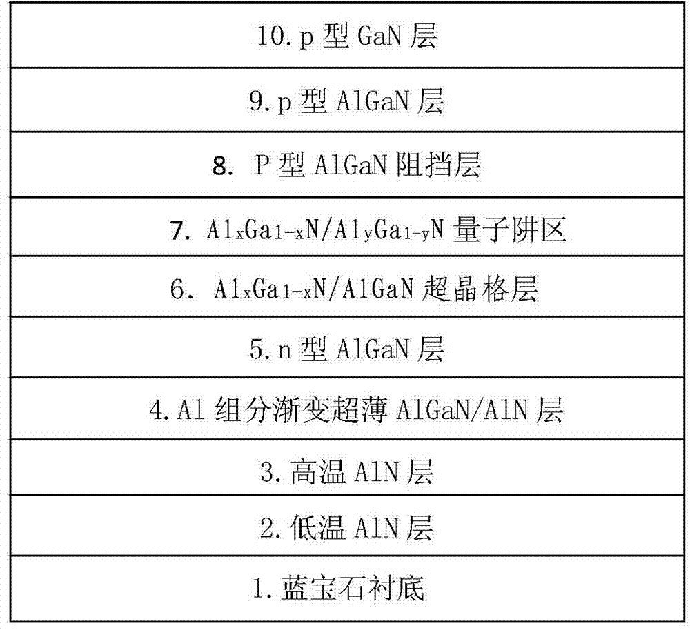
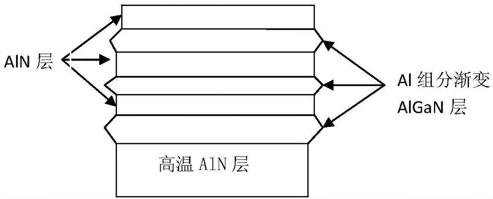
[0044] The present invention uses metal organic compound chemical vapor deposition (MOCVD) epitaxial growth technology, uses sapphire as the growth substrate, and performs heterogeneous epitaxial growth, using trimethylgallium (TMGa), triethylgallium (TEGa), and trimethylindium (TMIn), trimethylaluminum (TMAl) and ammonia (NH3) silane (SiH4) and dimagnesocene (cp2mg) respectively provide gallium source, indium source, aluminum source, and nitrogen source, silicon source, source of magnesium. like figure 1 , 2 As shown, the growth process of the ultraviolet LED epitaxy is as follows:

[0045] 1. After the sapphire substrate is specially cleaned, put it into the MOCVD equipment and bake it at 1100°C for 10 minutes.

[0046] 2. A low-temperature AlN layer with a thickness of 10 nm is grown at a temperature of 600° C., and the growth pressure is 150 torr.

[0047] 3. Raise the temperature to 1070°C to grow a high-temperature AlN layer with a thickness of 300nm, and the growth ...


PUM

PropertyMeasurementUnit
Thicknessaaaaaaaaaa

Abstract

The invention discloses a novel epitaxy method for growing an ultraviolet LED. The method can obviously improve the crystal quality of ultraviolet LED epitaxial growth materials and improve the light intensity of the ultraviolet LED. According to the method, an Al component gradient method is adopted to carry out doping in AlN, stress of crystal lattice adaption from a substrate layer can be released gradually, gradient component growth can reduce defects of crystal lattice adaption of an interface, the crystal quality of a material interface can be improved, slip dislocation can be carried out in gradient growth, penetration dislocation segregation is achieved, penetration dislocation is well stopped from entering a quantum well area, a quite good substrate is provided for growth of the quantum well, influences on quantum well growth caused by stress generated due to the crystal lattice adaption are reduced greatly, the integral crystal quality of materials is improved, the electron hole wave function spatial overlapping of a quantum well layer is enhanced, and optical and electrical properties of the whole ultraviolet LED are improved.

Description

technical field [0001] The invention belongs to the field of semiconductor optoelectronics, and in particular relates to a new violet LED epitaxy method. Background technique [0002] With the development of LED applications, the market demand for ultraviolet LEDs is increasing. Ultraviolet LEDs with emission wavelengths covering 210-400nm have advantages that traditional ultraviolet light sources cannot match. Ultraviolet LEDs can not only be used in the field of lighting, but also can replace traditional ultraviolet mercury lamps containing toxic and harmful substances in biomedicine, anti-counterfeiting identification, air and water purification, biochemical detection, and high-density information storage. Under the current LED background , the Ziguang market prospect is very broad. [0003] At present, the epitaxial growth technology of ultraviolet LED is not mature enough, and the material preparation for growing high-performance ultraviolet LED is difficult, and p-lay...

Claims


Application Information

Patent Timeline
IPC IPC(8): H01L33/04H01L33/00
CPCH01L33/007H01L33/04
Inventor 王晓波
Owner 西安利科光电科技有限公司
Why Eureka
Try Eureka