

Method for manufacturing graphene nanowire device
A technology of graphene nanometers and devices, which is applied in the field of preparing graphene nanowire devices, can solve the problems of inactive chemical properties and difficulties in depositing high-K dielectrics, and achieve the effects of small impact, reduced process steps, and reduced damage
- Summary
- Abstract
- Description
- Claims
- Application Information
AI Technical Summary
Problems solved by technology
Method used
Image


Examples
Embodiment Construction
[0018] In the invention, the nano groove is etched on the substrate to directly grow the required ultra-long graphene nanowire in the groove. Then, the dangling bonds of the silicon dioxide on the sidewall of the nano-groove are used to grow the high-K medium by the method of atomic layer deposition, and the nano-groove is filled with the high-K medium, so that the high-K medium physically covers the graphene, forming graphene. High K gate dielectric, which reduces damage to graphene. Described below is an embodiment of preparing a graphene nanowire device proposed by the present invention.
[0019] In the drawings, for convenience of explanation, the structural size and proportions do not represent the actual size.
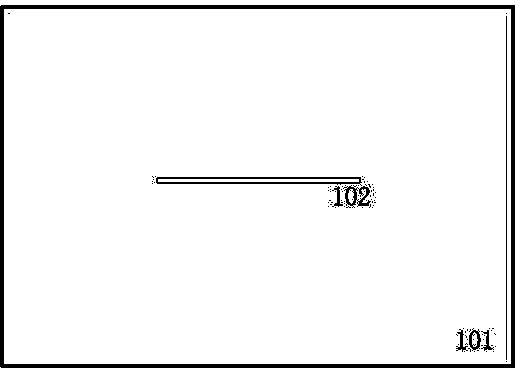
[0020] First, provide silicon dioxide (SiO 2 ) film sample 101, clean the sample, remove some magazines, particles, residual reagents, etc. on the surface of the sample, so that the graphene silica sample is very clean and tidy. Such as figure 2 shown.
[...
PUM
 Abstract
Description
Claims
Application Information