Surface plasma transmission device, manufacturing method and application
A technology of surface plasmon and transmission devices, which is applied in the direction of waveguide devices, cable/conductor manufacturing, electrical components, etc., can solve the problems that the transmission speed and transmission volume can not meet the requirements, can not transmit electrons at the same time, limitations, etc., to achieve structural Simple, small size, the effect of improving transmission speed and transmission volume
- Summary
- Abstract
- Description
- Claims
- Application Information
AI Technical Summary
Problems solved by technology
Method used
Image

Examples
Embodiment 1
[0028] Example 1 Preparation of silver nanowires
[0029] (1). Add 12ml EG (ethylene glycol) to the three-necked round-bottomed flask, stir magnetically (about 260rpm), heat to 150oC, and then heat to reflux at this temperature for 1h;
[0030] (2). Add 4ml AgNO to the three-necked round bottom flask within 10s 3 ethylene glycol solution (0.2M), then add 4ml of ethylene glycol solution of PVP K30 (22.2 mg / ml, PVP is the abbreviation of polyvinylpyrrolidone) within 5min, react for 1h, observe the white flocculent reactant, to stop the reaction. The longer the reaction time, the longer and thicker the obtained silver nanowires will be.
[0031] (3). In the reaction solution after step (2), add acetone (the volume ratio of the reaction solution to acetone is 1:3), carry out ultrasonic cleaning for 20min, centrifuge at 3000rpm for 20min, take the precipitate, add distilled water or ethanol to resuspend , 3000rpm centrifugation for 20min, repeated twice, and then added ethanol ...
Embodiment 2
[0033] Example 2 Preparation of Surface Plasmon Transport Device
[0034] (1). The silver nanowire ethanol suspension prepared in Example 1 was diluted with ethanol and used for later use.
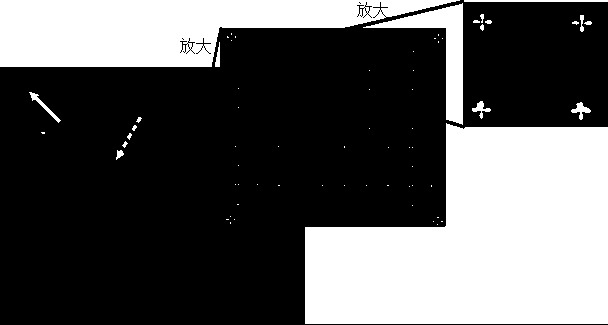
[0035] (2) Using a field emission scanning electron microscope, the designed mark pattern is etched on one side of the substrate by means of electron beam etching ( figure 2 ). The material of the substrate may be a glass substrate. The method of electron beam etching is as follows: spin coat a layer of resist with a thickness of about 350nm, the material is polymethyl methacrylate (PMMA), and dry at 170 °C; use the focused electron beam to etch the resist on the substrate Expose; sputter a gold conductive film with a thickness of about 20 nm; develop with a mixture of methyl isobutyl ketone and isoacetone (volume ratio of 1:3); deposit a 70 nm gold film by thermal evaporation; finally immerse In acetone, heated to 70°C, the gold film outside the marking pattern was peeled off to obta...
Embodiment 3
[0044] Example 3 Transmission performance of surface plasmon transport devices
[0045] 1. A method of synchronously transporting plasma and electrons
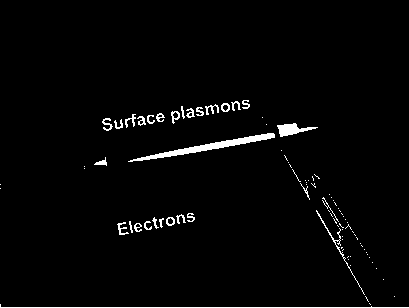
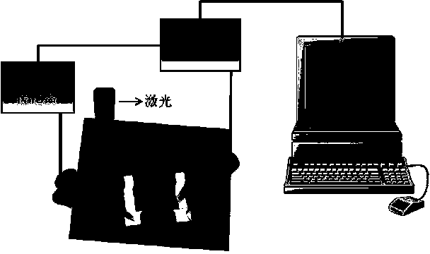
[0046] The surface plasmon transmission device prepared in Example 2 was placed on the sample stage of the leakage radiation microscope, and the silver nanowires and the two gold electrodes (numbered as A and B) connected to the silver nanowires were searched with the help of the microscope. The two probes connected to the voltage are connected to the gold electrodes A and B to form a series loop, so that the current passes through the silver nanowires. The specific process is as Figure 4 shown.
[0047] Above the silver nanowire, focusing the laser to one end of the silver nanowire can successfully excite surface plasmons in the silver nanowire. Depend on Figure 5 (a) Surface plasmons (bright lines on both sides of the nanowire) can be seen propagating in the nanowire connected to the gold electrode, and the bright spo...
PUM
| Property | Measurement | Unit |
|---|---|---|
| diameter | aaaaa | aaaaa |
| length | aaaaa | aaaaa |
| width | aaaaa | aaaaa |
Abstract
Description
Claims
Application Information
 - R&D
- Intellectual Property
- Life Sciences
- Materials
- Tech Scout
- Unparalleled Data Quality
- Higher Quality Content
- 60% Fewer Hallucinations
Browse by: Latest US Patents, China's latest patents, Technical Efficacy Thesaurus, Application Domain, Technology Topic, Popular Technical Reports.
© 2025 PatSnap. All rights reserved.Legal|Privacy policy|Modern Slavery Act Transparency Statement|Sitemap|About US| Contact US: help@patsnap.com