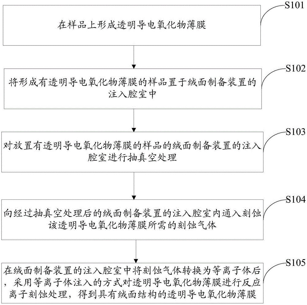
A kind of texturing method of transparent conductive oxide film
An oxide film, transparent and conductive technology, applied in the field of solar cells, can solve the problems of poor controllability and repeatability, impurity pollution, large difference in texture structure of TCO film, etc., to avoid poor controllability and strong reduction. The effect of anti-light trapping and improving photoelectric conversion performance
- Summary
- Abstract
- Description
- Claims
- Application Information
AI Technical Summary
Problems solved by technology
Method used
Image

Examples
example 1
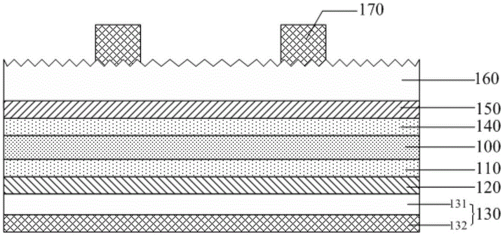
[0064] A silicon heterojunction solar cell, such as figure 2 As shown, it includes a crystalline silicon substrate 100, a first intrinsic amorphous silicon layer 110, an N-type amorphous silicon layer 120, and a back electrode 130 located on the backlight side of the crystalline silicon substrate 100 in sequence, and a crystalline silicon substrate 100 located in sequence The second intrinsic amorphous silicon layer 140, the P-type amorphous silicon layer 150, the first transparent conductive oxide film 160 and the gate line electrode 170 on the light incident side; wherein, the incident light of the first transparent conductive oxide film 160 The side has a textured structure, and the back electrode 130 is composed of a second transparent conductive oxide film 131 and a metal electrode 132 . In specific implementation, the preparation method of the above-mentioned silicon heterojunction solar cell specifically includes the following steps:
[0065] (1) cleaning the crystall...
example 2
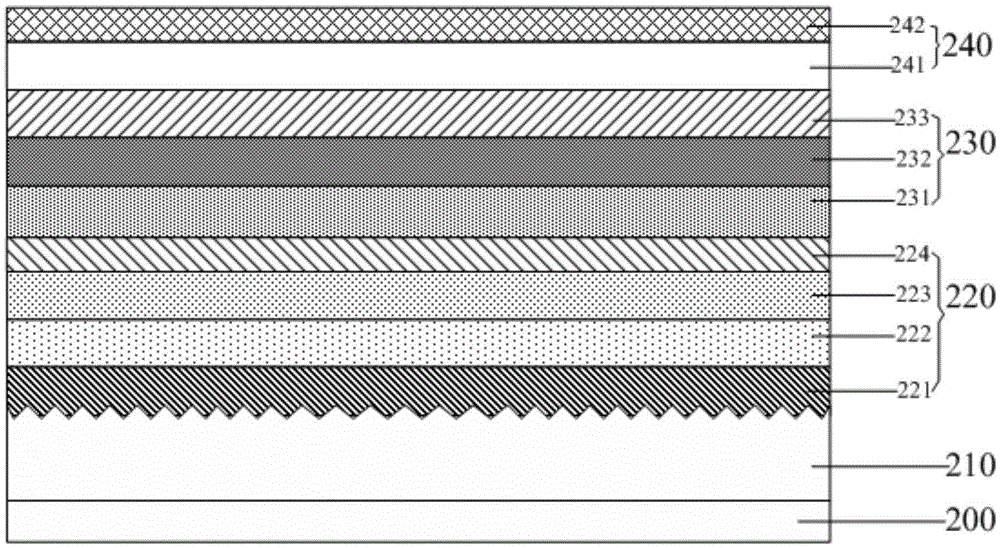
[0086] A silicon thin film solar cell, such as image 3 As shown, it includes a transparent substrate 200, a first transparent conductive oxide film 210, an amorphous silicon cell structure 220, a microcrystalline silicon cell structure 230, and a back electrode 240 located on one side of the transparent substrate 200 in sequence; wherein, the first The side of the transparent conductive oxide film 210 facing away from the transparent substrate 200 has a textured structure, and the amorphous silicon cell structure 220 includes a stacked transition layer 221, a P-type hydrogenated amorphous silicon layer (Pa-Si:H) 222, Intrinsic hydrogenated amorphous silicon layer (Ia-Si:H) 223 and N-type hydrogenated microcrystalline silicon layer (Nμc-Si:H) 224, the microcrystalline silicon cell structure 230 includes a stacked P-type hydrogenated microcrystalline silicon layer (Pμc-Si:H) 231, intrinsic hydrogenated microcrystalline silicon layer (Iμc-Si:H) 232 and N-type hydrogenated amorph...
PUM
 Abstract
Description
Claims
Application Information
PatSnap Eureka turns technology decisions into work you can execute. Powered by our Innovation Knowledge Graph, it runs expert workflows across engineering, life sciences, materials and intellectual property. Get your review-ready output in minutes.


