GaN-based ultraviolet avalanche photo-detector

A photodetector and ultraviolet avalanche technology, applied in circuits, electrical components, semiconductor devices, etc., can solve the problem of difficult tuning of device cut-off wavelength, and achieve high lateral carrier mobility, high absorption coefficient, and strong polarization effect Effect

A photodetector and ultraviolet avalanche technology, applied in circuits, electrical components, semiconductor devices, etc., can solve the problem of difficult tuning of device cut-off wavelength, and achieve high lateral carrier mobility, high absorption coefficient, and strong polarization effect Effect

CN104051561AInactive Publication Date: 2014-09-17SOUTHEAST UNIV

Image

  • GaN-based ultraviolet avalanche photo-detector

Examples


Embodiment Construction

[0021] The present invention will be further described below in conjunction with the accompanying drawings.

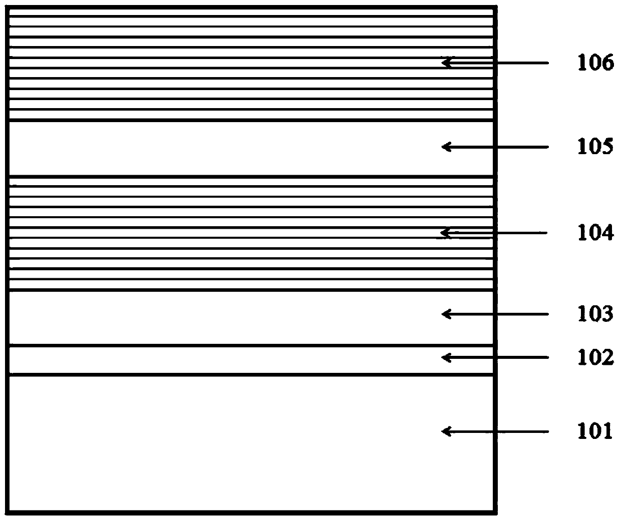
[0022] like figure 1 Shown is a gallium nitride-based ultraviolet avalanche photodetector, including a sapphire substrate 101, a low-temperature nucleation layer 102, and an n-type Al composition graded Al x In y Ga 1-x-y N layer 103, Al x1 In y1 Ga 1-x1-y1 N / Al x2 In y2 Ga 1-x2-y2 N multi-quantum well structure absorption region 104, Al composition graded Al x3 In y3 Ga 1-x3-y3 N layer 105 and Al x4 In y4 Ga 1-x4-y4 N / Al x5 In y5 Ga 1-x5-y5 N multiple quantum well structure multiplication region 106, where Al x1 In y1 Ga 1-x1-y1 N / Al x2 In y2 Ga 1-x2-y2 N multi-quantum well structure absorption region 104 and Al x4 In y4 Ga 1-x4-y4 N / Al x5 In y5 Ga 1-x5-y5 The multiplication region 106 of the N multiquantum well structure serves as the absorption region and the multiplication region of the gallium nitride-based ultraviolet avalanche photode...


PUM


Abstract

The invention discloses a GaN-based ultraviolet avalanche photo-detector. The GaN-based ultraviolet avalanche photo-detector is formed by arranging a sapphire substrate, a low-temperature nucleation layer, an n-type Al component gradient AlxInyGa1-x-yN layer, an Alx1Iny1Ga1-x1-y1N / Alx2Iny2Ga1-x2-y2N multi-quantum well structure absorption region, an Al component gradient Alx3Iny3Ga1-x3-y3N layer and an Alx4Iny4Ga1-x4-y4N / Alx5Iny5Ga1-x5-y5N multi-quantum well structure multiplication region in sequence from bottom to top. As a multi-quantum well has the advantages of high absorption coefficients, high transverse carrier mobility, strong polarization effects and the like, the absorption region and the multiplication region of the GaN-based ultraviolet avalanche photo-detector are designed to be of a multi-quantum well structure. In this way, the quantum efficiency and responsivity of the GaN-based ultraviolet avalanche photo-detector can be enhanced, the cut-off wavelength of the photo-detector can be freely tuned, and meanwhile the threshold value of avalanche breakdown voltage can be effectively reduced. Accordingly, important significance is achieved for manufacturing the high-performance ultraviolet photo-detector.

Description

technical field [0001] The invention relates to a GaN-based ultraviolet avalanche photodetector with multiple quantum well structure absorption regions and multiplication regions, belonging to the technical field of semiconductor optoelectronic materials and device manufacturing. Background technique [0002] Gallium nitride-based materials mainly include binary compounds GaN, InN, and AlN of group III and group V elements, ternary compounds InGaN, AlGaN, AlInN and quaternary compounds AlInGaN, which have large band gap, high thermal conductivity, and high temperature resistance. , anti-radiation, acid and alkali resistance, high strength and high hardness and other characteristics, it has a wide range of applications in the fields of high-brightness blue, green, purple, ultraviolet and white light diodes, blue and violet lasers, radiation resistance, high temperature resistance, high-power microwave devices, etc. Application potential and good market prospect. Ternary comp...

Claims


Application Information

Patent Timeline
17 Sep 2014
Publication
CN104051561A
IPC
H01L31/107; H01L31/0352; H01L31/0304
CPC
H01L31/03048; H01L31/035236; H01L31/107
Inventors
εΌ ι›„; 杨ζ΄ͺ权