Chemical vapor deposition method for preparing graphene
A chemical vapor deposition and graphene technology, applied in the field of graphene preparation, can solve problems such as loss of electrical conductivity, low graphene quality, and difficulty in reducing graphite, and achieve the effects of less energy consumption, high light transmittance, and low substrate temperature.
- Summary
- Abstract
- Description
- Claims
- Application Information
AI Technical Summary
Problems solved by technology
Method used
Image
Examples
Embodiment 1
[0027] Present embodiment provides a kind of chemical vapor deposition method to prepare graphene, is to make through the following steps:
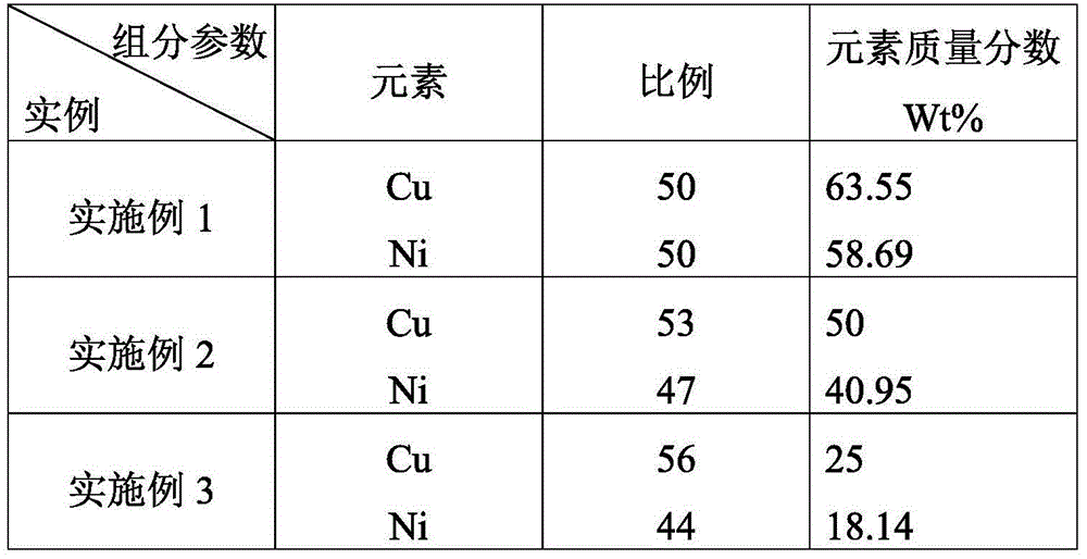
[0028] Step 1. Select monocrystalline silicon as the substrate. The monocrystalline silicon substrate is ultrasonically cleaned in acetone, absolute ethanol, and deionized water for 18 to 20 minutes, and then dried in a nitrogen environment. Copper and nickel double-target magnetron co-sputtering method The vacuum degree at the back of the sputtering chamber is 5.0×10 -4 , the argon gas flow rate is 20sccm, the sputtering time is 30min, the sputtering pressure is 1.0Pa, the sputtering power of copper target is 120W, and the sputtering power of nickel target is 90W, and the thickness of 4μm copper-nickel alloy film is prepared on the surface of single crystal silicon ;
[0029] Step 2, the single crystal silicon substrate that the surface is deposited with copper-nickel alloy thin film is transferred in the reaction furnace of chemical va...
Embodiment 2
[0038] Present embodiment provides a kind of chemical vapor deposition method to prepare graphene, is to make through the following steps:
[0039] Step 1. Select monocrystalline silicon as the substrate. The monocrystalline silicon substrate is ultrasonically cleaned in acetone, absolute ethanol, and deionized water for 18 to 20 minutes, and then dried in a nitrogen environment. Copper and nickel double-target magnetron co-sputtering method The vacuum degree at the back of the sputtering chamber is 5.0×10 -4 , the argon gas flow rate is 20sccm, the sputtering time is 30min, the sputtering pressure is 1.0Pa, the sputtering power of copper target is 135W, and the sputtering power of nickel target is 90W, and the thickness of 4μm copper-nickel alloy film is prepared on the surface of single crystal silicon ;
[0040] Step 2, the single crystal silicon substrate that the surface is deposited with copper-nickel alloy thin film is transferred in the reaction furnace of chemical va...
Embodiment 3
[0049] Present embodiment provides a kind of chemical vapor deposition method to prepare graphene, is to make through the following steps:
[0050] Step 1. Select monocrystalline silicon as the substrate. The monocrystalline silicon substrate is ultrasonically cleaned in acetone, absolute ethanol, and deionized water for 18 to 20 minutes, and then dried in a nitrogen environment. Copper and nickel double-target magnetron co-sputtering method The vacuum degree at the back of the sputtering chamber is 5.0×10 -4 , the argon gas flow rate is 20sccm, the sputtering time is 30min, the sputtering pressure is 1.0Pa, the sputtering power of copper target is 150W, and the sputtering power of nickel target is 90W, and the thickness of 4μm copper-nickel alloy film is prepared on the surface of single crystal silicon ;
[0051] Step 2, the single crystal silicon substrate that the surface is deposited with copper-nickel alloy thin film is transferred in the reaction furnace of chemical va...
PUM
 Abstract
Description
Claims
Application Information

