White light top emission type OLED (organic light emitting diodes) and preparation method thereof

A light-emitting diode, top-emitting technology, applied in semiconductor/solid-state device manufacturing, electrical components, electrical solid-state devices, etc., can solve the problems of low luminous efficiency of blue light-emitting materials, achieve simple preparation process, reduce angle dependence, improve The effect of efficiency

Inactive Publication Date: 2014-10-29
NANJING UNIV OF POSTS & TELECOMM
View PDF2 Cites 9 Cited by
  • Summary
  • Abstract
  • Description
  • Claims
  • Application Information

AI Technical Summary

Problems solved by technology

In addition, the luminous efficiency of the blue light-emitting material itself is low, so the key to realizing a high-performance white TOLED is to increase the intensity of blue light in the device[8,9] ([8] P. Freitag, S. Reineke, S. Olthof, M. Furno, B. Lussem, K. Leo, Org. Electron., 2010, 11, 1676 .[9] L. L. Deng, S. F. Chen, J. Xie, Q. Yan, Org. Electron. , 2013, 14, 423.)

Method used


Image

  • White light top emission type OLED (organic light emitting diodes) and preparation method thereof
  • White light top emission type OLED (organic light emitting diodes) and preparation method thereof
  • White light top emission type OLED (organic light emitting diodes) and preparation method thereof

Examples


Embodiment 1

[0035] 1) Clean the glass substrate as the substrate 1;

[0036] 2) After putting the glass substrate into the vacuum evaporation chamber, vacuumize to 5×10 -4 Above Pa; 3) Evaporate metal Ag reflective anode 2 at a deposition rate of 0.1 nm / S, with a thickness of 80 nm;

[0037] 4) Evaporation of hole injection layer 3: First, use a single-component organic material MoOx to evaporate the MoOx layer, wherein the deposition rate is 0.1 nm / S, the evaporation thickness is 2 nm, cool for 30 minutes, and then use a single-component organic material m- MTDATA evaporated the m-MTDATA layer with a deposition rate of 0.1 nm / S and a thickness of 25 nm; evaporated the hole transport layer 4 with a single-component organic material to evaporate the NPB layer with a deposition rate of 0.1 nm / S and evaporated Plating thickness is 15 nm;

[0038] 5) Evaporate the double blue light-emitting layer 5, first use the hole-type host material TCTA: the blue-light guest material FIrpic with a mass...

Embodiment 2

[0047] 1) Same as in Example 1, clean the glass substrate substrate 1, reflective anode 2, hole injection layer 3, hole transport layer 4, double blue light emitting layer 5, red light emitting layer 6, electron transport layer 7 , the evaporation of the electron injection layer 8 and the translucent cathode 9;

[0048] 2) The vapor-deposited light coupling output layer 10 is formed by vapor-depositing the single-component organic material m-MTDATA, with a thickness of 60 nm.

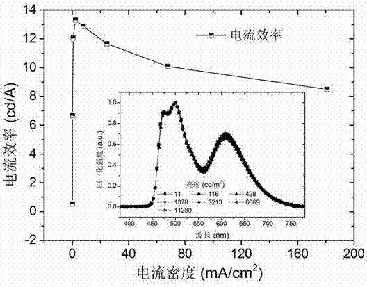
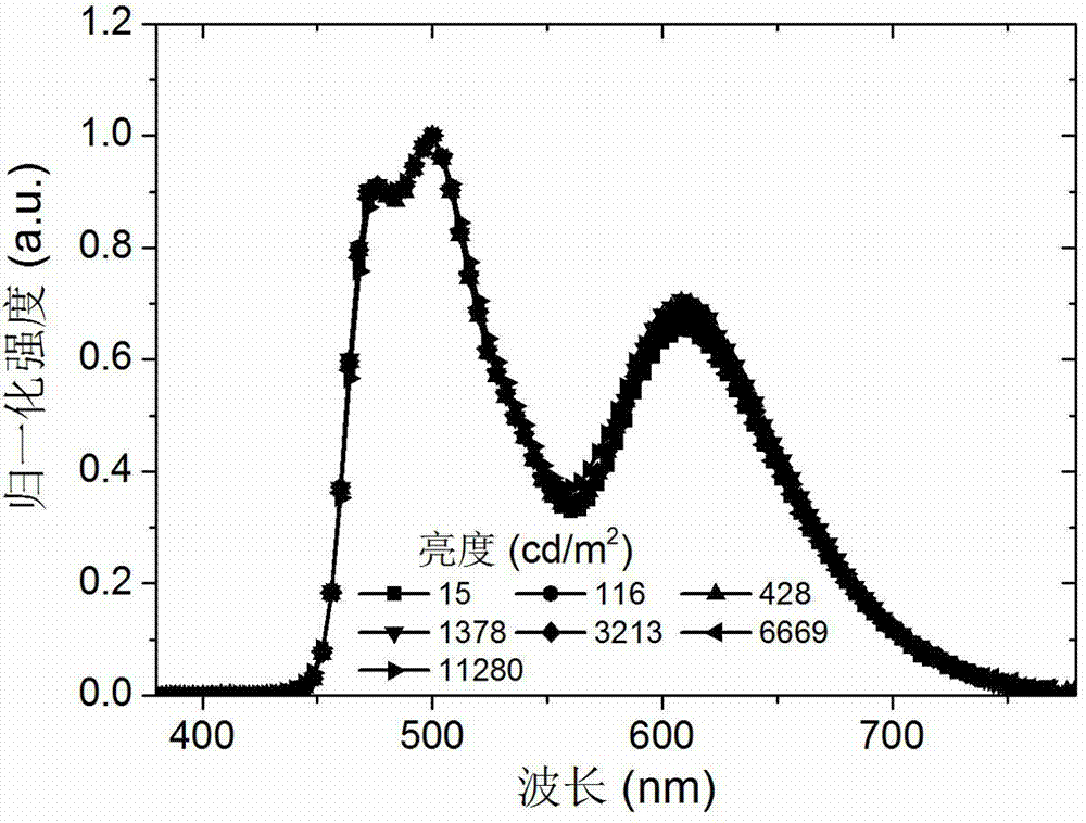
[0049] Compared with Example 1, the optical outcoupling layer of the device in Example 2 is increased to 60 nm. For m-MTDATA as the coupling output material, 60 nm is the optimal thickness, which can maximize the light output and improve the device efficiency. Through the improvement of this structure, the maximum brightness of the device in Example 2 reaches 18940 cd / m 2 , the maximum efficiency reaches 16.6 cd / A, the color coordinates are (0.31, 0.44), and the color coordinates drift during the whol...

Embodiment 3

[0052]1) Same as Example 1, cleaning of the glass substrate substrate 1, evaporation of the reflective anode 2, the hole injection layer 3, the hole transport layer 4, the double blue light emitting layer 5 and the red light emitting layer 6;

[0053] 2) The electron injection layer 8 is evaporated, and the electron transport material BPhen is used: the mass percentage is 2% Li evaporated, and the thickness is 20 nm;

[0054] 3) The same as in Example 1, conduct evaporation of the translucent cathode 9 and the optical coupling output layer 10;

[0055] 4) The current-voltage-luminance and spectral characteristics of the device are measured by Keithley2400 current source combined with PR-655 spectrometer.

[0056] Compared with Example 1, the doping concentration of Li in the electron injection layer of the device in Example 3 was reduced to 2%. Due to the reduction of electron concentration, the efficiency and chromaticity of the device are slightly changed. The device in Ex...


PUM


Abstract

Disclosed is a white light top emission type OLED and a preparation method thereof. A substrate, a reflective anode, a hole injection layer, a hole transport layer, a double blue light luminous layer, a red light luminous layer, an electron transfer layer, an electron injection layer, a semitransparent cathode and an optical coupling output layer are sequentially evaporated from bottom to top. The preparation process comprises firstly cleaning the substrate, then performing evaporation in vacuum and cooling after the evaporation is finished. The preparation method of white light top emission type OLED effectively restrains multi-beam interference by means of the semitransparent cathode and the optical coupling output layer, thereby enhancing output of white light on the whole; enhances wide-angle interference of a blue light blue light waveband through a structural feature that the double blue light luminous layer is adjacent to the anode; utilizes the double blue light luminous layer of a heterojunction structure to control an exciton recombination region for increasing intensity of blue light as well as improving stability of chroma of a device; effectively improves the chroma and the stability of the white light top emission type OLED, thereby having potential application values.

Description

technical field [0001] The invention relates to the technical field of organic electroluminescence, in particular to a white top-emission organic light-emitting diode and a preparation method thereof. Background technique [0002] Organic light-emitting diodes (OLEDs) have become the most promising new-generation light-emitting technology because of their advantages such as all-solid-state, active light-emitting, high brightness, low power consumption, high luminous efficiency, wide operating temperature, and flexibility. White light OLED can not only realize full-color display, but also can be used as a lighting source and a backlight source for liquid crystal display, which has set off a research boom in academia and industry [1,2] ([1] C. W. Tang, S. A. Van Slyke, Appl. Phys. Lett., 1987, 51, 913. [2] G. Gustufsson, Y. Cao, G. M. Treacy, F. Klavetter, N. Colaneri, A. J. Heeger, Nature , 1992, 357, 447.). Traditional white OLEDs are bottom-emission, that is, light is emi...

Claims


Application Information

Patent Timeline
Patent Type & Authority Applications(China)
IPC IPC(8): H01L51/52H01L51/54H01L51/56
CPCH10K50/11H10K50/805H10K50/85H10K71/00
Inventor 邓玲玲陈淑芬石弘颖刘斌黄维
Owner NANJING UNIV OF POSTS & TELECOMM
Why Eureka
Try Eureka