Gallium-nitride-based heterostructure field effect transistor with composite barrier layers

A heterojunction field effect and composite barrier technology, applied in semiconductor devices, electrical components, circuits, etc., can solve the problems of device output current drop, reaction speed drop, current collapse effect, etc., to increase drift speed and improve endurance The effect of pressure and simple process

Active Publication Date: 2014-12-10
UNIV OF ELECTRONICS SCI & TECH OF CHINA
View PDF6 Cites 17 Cited by
  • Summary
  • Abstract
  • Description
  • Claims
  • Application Information

AI Technical Summary

Problems solved by technology

However, due to the lattice mismatch, the back barrier will introduce traps between the buffer layer and the channel, which will also cause disadvantages such as device output current drop, current collapse effect, and reaction speed drop.

Method used


Image

  • Gallium-nitride-based heterostructure field effect transistor with composite barrier layers
  • Gallium-nitride-based heterostructure field effect transistor with composite barrier layers
  • Gallium-nitride-based heterostructure field effect transistor with composite barrier layers

Examples


Embodiment 1

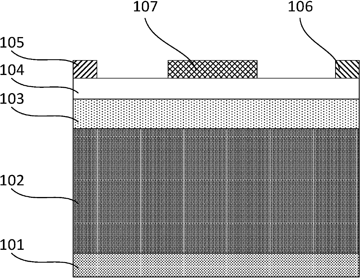
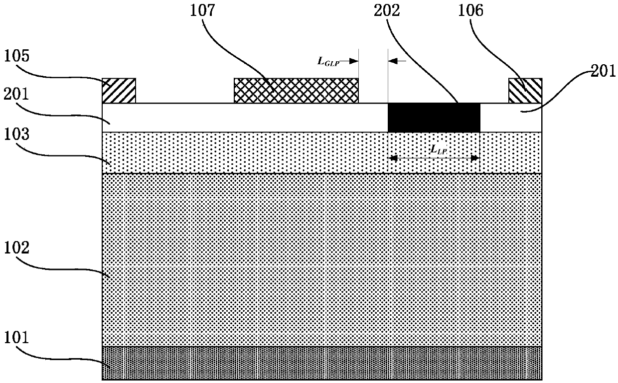
[0037] This example is used as a power device. like figure 2 As shown, the GaN HEMT of this example includes a substrate 101, a gallium nitride buffer layer 102 disposed on the substrate 101, a gallium nitride channel layer 103 disposed on the gallium nitride buffer layer 102, a source 105, a drain Pole 106 and gate 107; It is characterized in that, a compound barrier layer is arranged on the upper layer of the gallium nitride channel layer 103, and the source electrode 105 and the drain electrode 106 are located at both ends of the upper surface of the compound barrier layer and are connected to the compound potential The barrier layer forms an ohmic contact, and the grid 107 is located in the middle of the upper surface of the composite barrier layer and forms a Schottky contact with the composite barrier layer; the composite barrier layer is composed of a high polarization barrier layer 201 and a low pole The two ends of the low polarization barrier layer 202 are connecte...

Embodiment 2

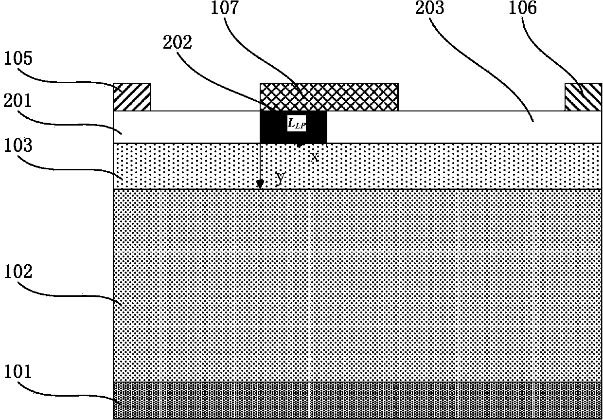
[0047] This example is used as a microwave device. like image 3 As shown, the GaN HEMT structure of this example differs from Embodiment 1 in that the low polarization barrier layer 202 in the composite barrier layer is located in the area directly below the gate, the left edge is aligned with the source end of the gate, and the right edge is not beyond the gate drain terminal. The main process steps of the GaN HEMT provided in this embodiment are as follows: First, a gallium nitride (GaN) buffer layer 102 and a gallium nitride (GaN) channel layer 103 are sequentially grown on the substrate by MOCVD, and then grown by selective growth technology Growing a high-polarization barrier layer 201 and a low-polarization barrier layer 202 with different polarization strengths to form a composite barrier layer; finally, forming a source electrode 105 and a drain electrode 106 in ohmic contact with the composite barrier layer , and a gate 107 in Schottky contact with the barrier laye...


PUM


Abstract

The invention discloses a gallium-nitride-based heterostructure field effect transistor with composite barrier layers. The composite barrier layers are formed by AlInGaN material with different polarization intensities. When the AlInGaN composite barrier layer with low polarization intensity is located at a grid drain terminal, the density of two-dimensional electron gas (2DEG) of the channel below the barrier layer is smaller than that of the 2DEG at other positions of the channel drain terminal, an LDD structure is formed, and the electric field distribution of the channel is modulated to increase voltage endurance capability; when the AlInGaN composite barrier layer with low polarization intensity is located right below a grid, a below-grid gallium nitride (GaN) channel guide strip bottom is distributed in a stepped manner, the drift speed of a below-grid channel carrier is increased due to barrier descending, electric field peak is generated between AlInGaN composite barrier layer with two different elemental components, and more potential is distributed at the grid drain terminal instead of the whole grid to restrain drain induced barrier lowering (DIBL).

Description

technical field [0001] The invention belongs to the technical field of semiconductors, and in particular relates to a gallium nitride-based heterojunction field effect transistor with a composite barrier layer. Background technique [0002] Gallium nitride (GaN) based heterojunction field effect transistor has excellent characteristics such as large band gap, high critical breakdown electric field, high electron saturation velocity, good thermal conductivity, radiation resistance and good chemical stability. (GaN) materials can form two-dimensional electron gas heterojunction channels with high concentration and high mobility with materials such as aluminum gallium nitride (AlGaN), so they are especially suitable for high-voltage, high-power and high-temperature applications, and are the most suitable for power electronics applications. One of the most promising transistors. [0003] figure 1 It is a schematic diagram of a traditional GaN HFET structure based on the prior ...

Claims


Application Information

Patent Timeline
Patent Type & Authority Applications(China)
IPC IPC(8): H01L29/778H01L29/06H01L29/10
CPCH01L29/1054H01L29/7786
Inventor 杜江锋潘沛霖陈南庭刘东于奇
Owner UNIV OF ELECTRONICS SCI & TECH OF CHINA
Why Eureka
Try Eureka