Organic light emission diode device and fabrication method thereof

An electroluminescent device and luminescent technology, which is applied in the direction of electric solid-state devices, semiconductor/solid-state device manufacturing, electrical components, etc., can solve the problems of low light-emitting performance, total reflection loss, and low transmittance of light-emitting devices, and achieve luminescence Excellent efficiency, increased light extraction efficiency, and high light extraction efficiency

Inactive Publication Date: 2014-12-17
OCEANS KING LIGHTING SCI&TECH CO LTD +2
View PDF5 Cites 4 Cited by
  • Summary
  • Abstract
  • Description
  • Claims
  • Application Information

AI Technical Summary

Problems solved by technology

[0003] In traditional top-emitting OLED light-emitting devices, the cathode used is generally a thin layer of metal, and its transmittance is low, generally only about 50%. In addition, due to the difference in refractive index between the interface layers of the device, it causes The loss of total refle...

Method used


Image

  • Organic light emission diode device and fabrication method thereof
  • Organic light emission diode device and fabrication method thereof
  • Organic light emission diode device and fabrication method thereof

Examples


Embodiment 1

[0058] A method for preparing an organic electroluminescent device, comprising the following steps:

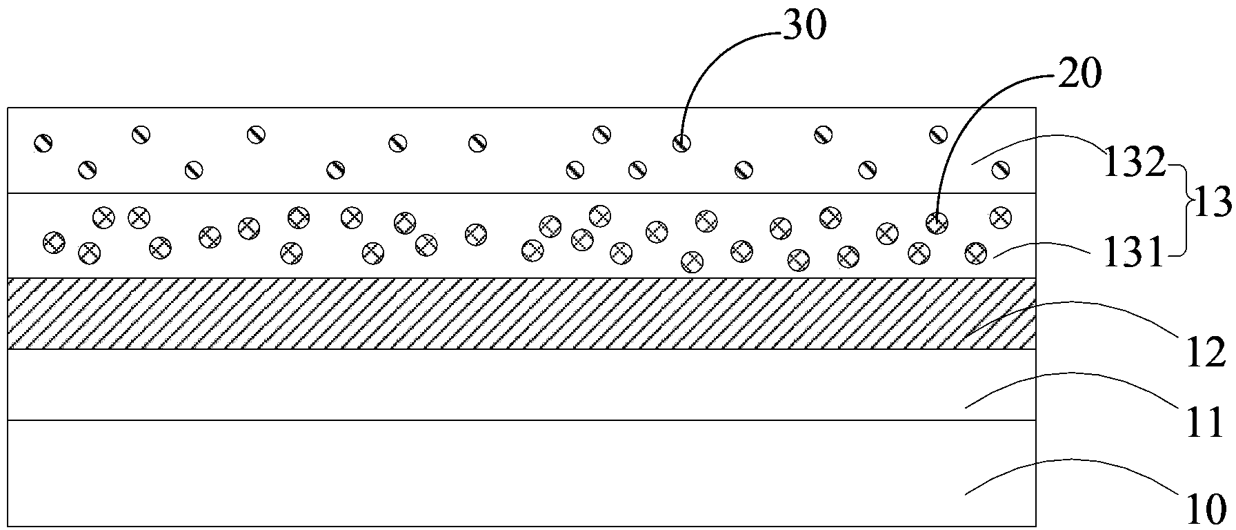
[0059] (1) Place a transparent glass substrate on a 1×10 -4 In the vacuum coating chamber of Pa, a metal Ag thin film with a thickness of 100nm is prepared on the surface of the substrate as an anode by means of vacuum thermal resistance evaporation;

[0060] (2) Prepare a light-emitting functional layer on the surface of the metal Ag thin film by vacuum thermal resistance evaporation, including a hole injection layer, a hole transport layer, a light-emitting layer, an electron transport layer, and an electron injection layer in sequence;

[0061] Among them, the hole injection layer is made of CuPc with a thickness of 20nm, the hole transport layer is made of NPB with a thickness of 30nm, and the light emitting layer is made of Alq 3 , the thickness is 15nm, and then the electron transport layer is made of TPBi with a thickness of 30nm, and the electron injection layer is ma...

Embodiment 2

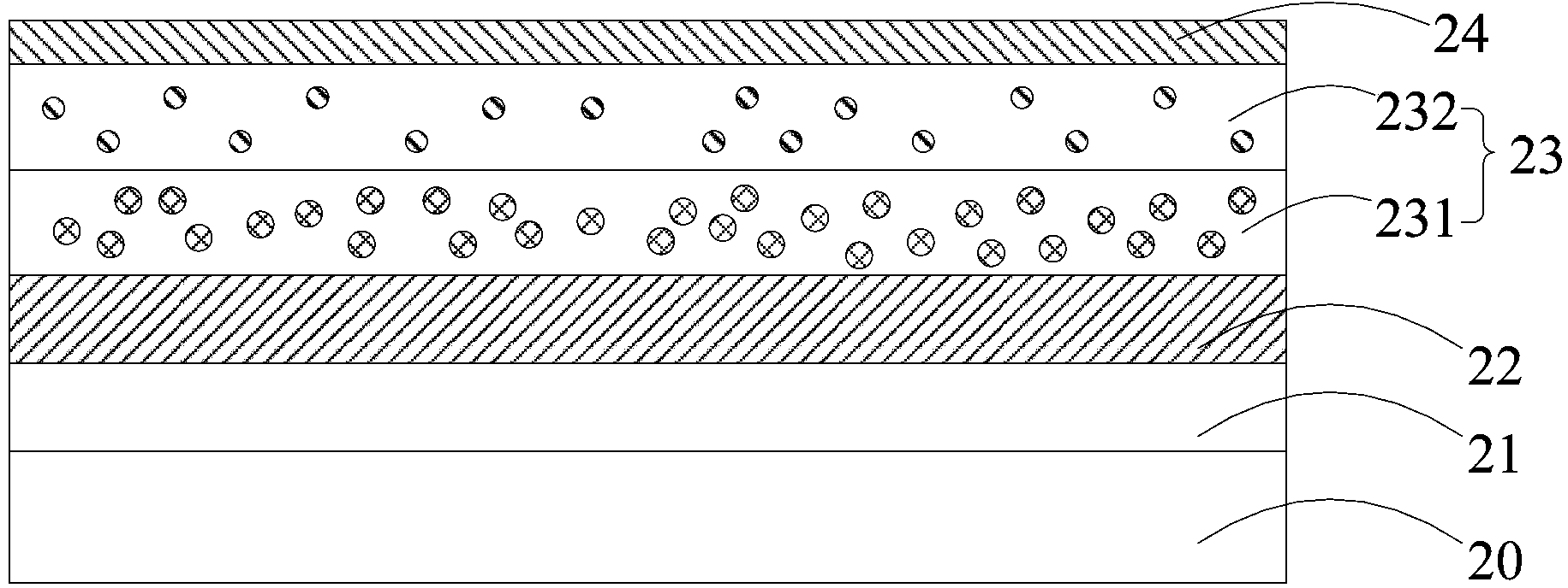
[0067] The difference between this embodiment and Embodiment 1 is that the thickness of the first doped layer is 40nm, and the SiO in the second doped layer 2 The mass ratio to metal Au is 10:100, namely SiO 2 The ratio of the evaporation rate to the metal Au is 10:100, where SiO 2 The evaporation rate of Au is 0.2nm / s, and the evaporation rate of Au is 2nm / s.

Embodiment 3

[0069] The difference between this embodiment and Embodiment 1 is that the thickness of the first doped layer is 40nm, and the SiO in the second doped layer 2 The mass ratio to metal Au is 100:100, namely SiO 2 The ratio to the evaporation rate of metal Au is 100:100, where SiO 2 The evaporation rate of Au is 1 nm / s, the evaporation rate of Au is 1 nm / s, and the thickness of the second doped layer is 100 nm.


PUM

PropertyMeasurementUnit
Particle sizeaaaaaaaaaa
Thicknessaaaaaaaaaa
Thicknessaaaaaaaaaa

Abstract

The invention provides an organic light emission diode device which comprises a substrate, an anode, a light emission functional layer and a cathode, the cathode comprises a first doping layer and a second doping layer which are sequentially laminated, the material of the first doping is a mixed material formed by organic particles and metal, the mass rate of the organic particles to the metal is (0.6-1.2):1, the grain size of the organic particles is 10 to 100 nanometers, the organic particles are an electron-transmitted organic material, the material of the second doping layer is a mixed material formed by inorganic particles and metal, the mass rate of the inorganic particles to the metal is (0.02-1):1, the grain size of the inorganic particles is 10 to 50 nanometers, the inorganic particles are one or more of silicon monoxide, silicon dioxide, titanium dioxide and tungsten oxide, and the metal is elementary substance of gold, silver, aluminum or magnesium. The luminous efficiency of the cathode of the organic light emission diode device is high, therefore, the luminous efficiency of the device is improved. The invention also provides a fabrication method of the organic light emission diode device.

Description

technical field [0001] The invention relates to an organic electroluminescent device, in particular to an organic electroluminescent device and a preparation method thereof. Background technique [0002] Organic Light Emission Diode, hereinafter referred to as OLED, has the characteristics of high brightness, wide range of material selection, low driving voltage, fully cured active light emission, etc., and has the advantages of high definition, wide viewing angle, and fast response speed. It is a display technology and light source with great potential, which conforms to the development trend of mobile communication and information display in the information age, as well as the requirements of green lighting technology, and is the focus of many researchers at home and abroad. [0003] In traditional top-emitting OLED light-emitting devices, the cathode used is generally a thin layer of metal, and its transmittance is low, generally only about 50%. In addition, due to the di...

Claims


Application Information

Patent Timeline
IPC IPC(8): H01L51/50H01L51/52H01L51/54H01L51/56
CPCH10K71/164H10K50/165H10K50/11H10K71/00
Inventor 周明杰冯小明黄辉王平
Owner OCEANS KING LIGHTING SCI&TECH CO LTD
Why Eureka
Try Eureka