Silicon single crystal and method for manufacture thereof

A manufacturing method and technology of single crystal silicon, applied in the direction of single crystal growth, single crystal growth, chemical instruments and methods, etc., can solve the problems of high temperature, high cost, poor crystallization yield, etc.

Active Publication Date: 2015-01-14
GLOBALWAFERS JAPAN
View PDF2 Cites 22 Cited by
  • Summary
  • Abstract
  • Description
  • Claims
  • Application Information

AI Technical Summary

Problems solved by technology

[0014] However, in the method described in the above-mentioned Patent Document 1, the cost of coating SiC or the like on the high-temperature carbon member is very high.
In addition, since the side heaters around the crucible become extremely hot, the coated SiC may be peeled off after several times of pulling, making it unsuitable for mass production.
[0015] Furthermore, in this method, when the solidification rate of the crystal is 55% or more, the carbon concentration becomes 1.0×10 14 atoms / cm 3 As above, the yield difference that can be used as a crystal for high voltage IGBT
In addition, the oxygen concentration is 1.3×10 18 atoms / cm 3 In the case of above, oxygen precipitation and nucleation will grow, so it is not suitable for silicon substrates for high-voltage IGBTs.
[0016] On the other hand, in the method described in the above-mentioned Patent Document 2, in order to raise the temperature of the silicon melt and keep it at a high temperature, it is necessary to increase the power of the heater. The speed of pollution mixed into the silicon melt becomes an advantage, and the carbon concentration in the pulled crystals will increase instead.
[0017] In addition, the evaporation rate of CO from silicon melt is very small compared with that of SiO from silicon melt, so even if the evaporation rate of CO in silicon melt becomes more dominant than the contamination rate, in order to make the The carbon concentration is reduced to 1×10 14 atoms / cm 3 Next, a very long decarburization step is also required, resulting in a decrease in productivity

Method used


Image

  • Silicon single crystal and method for manufacture thereof
  • Silicon single crystal and method for manufacture thereof
  • Silicon single crystal and method for manufacture thereof

Examples


Embodiment 1

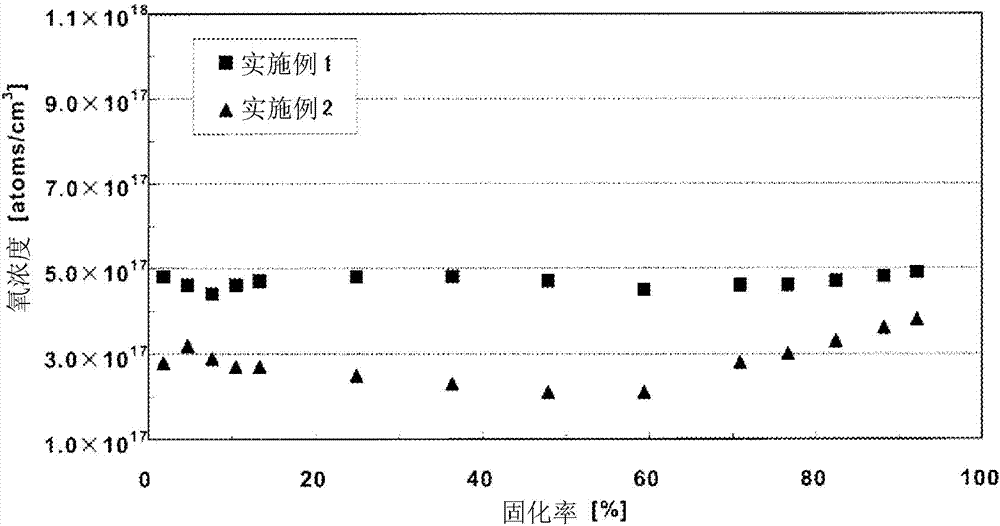
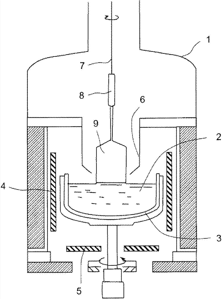
[0091] in figure 1 In the single crystal pulling device using the CZ method shown, 10 single crystal silicon are pulled so that the crystal diameter of the straight body portion is 200 mm, and the solidification rate of the crystal at the end of the straight body portion reaches 90%.

[0092] The carbon concentration used in raw materials is about 5.0×10 14 atoms / cm 3 Of polysilicon.

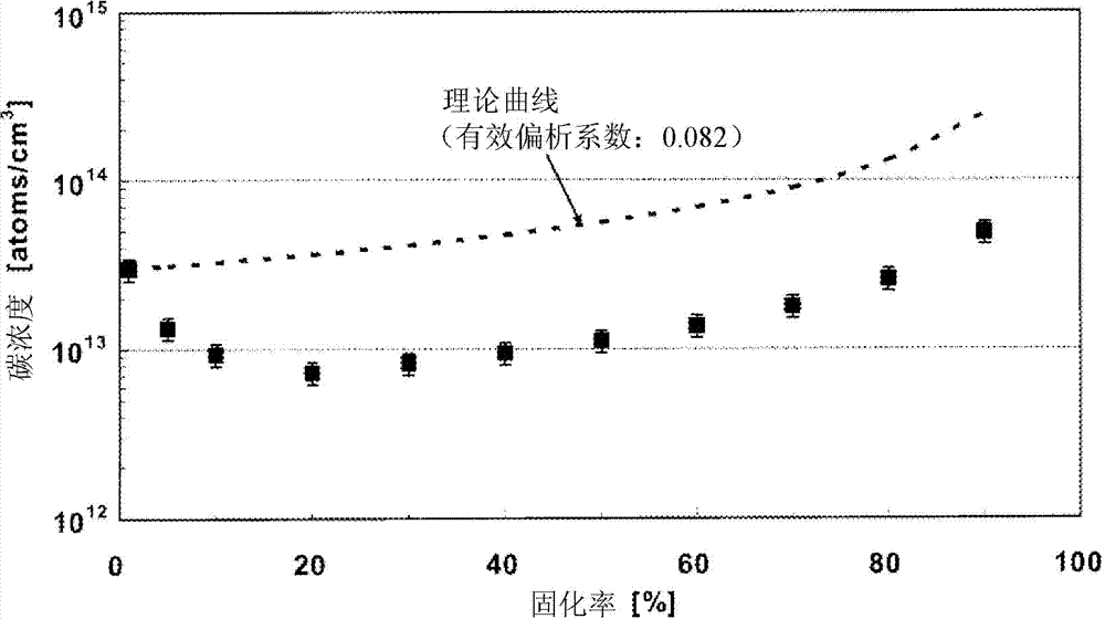
[0093] As the pulling conditions, a transverse magnetic field is applied to the raw material melt during crystal pulling, the rotation speed of the quartz crucible filled with the raw material melt is 0.1 to 1.0 rpm, and the crystal rotation speed is controlled in the range of 15 to 25 rpm, so that The pulling speed of the crystal straight body part is 1.0-1.3mm / min. It should be noted that the effective segregation coefficient calculated by considering these working conditions is 0.082.

[0094] In addition, the flow rate Q of argon gas is 150 L / min, the pressure P in the furnace is 30 Torr, the open...

Embodiment 2

[0101] The distance Y from the surface of the raw material melt to the lower end of the radiation shield is 40mm, the flow rate Q of argon is 80L / min, the pressure P in the furnace is 50 Torr, and the opening diameter X of the radiation shield is 250mm. At a position 8-20 mm above the surface of the raw material melt, at least the flow rate A of argon gas from the beginning of the melting of the raw material until the solidification rate of the pulled crystal reaches 30% is 0.2-25 m / sec. In addition, The reduction rate of the total power of the side heater and the bottom heater from when the seed crystal comes into contact with the aforementioned raw material melt until the solidification rate of the pulled crystal reaches 30%, the side heater Except for the reduction rate of power of 13%, 10 pieces of single crystal silicon were pulled in the same manner as in Example 1, and the carbon concentration was measured. The graph of the relationship between the carbon concentration a...


PUM


Abstract

A silicon single crystal manufacturing method includes: applying a transverse magnetic field to a melt of polysilicon with a carbon concentration of at most 1.0 × 10 15 atoms / cm 3 as a raw material; rotating the crucible at 5.0 rpm or less; allowing inert gas to flow at rate A (m / sec) of formula (1) at a position 20-50% of Y above the melt surface; controlling the rate A within the range of 0.2 to 5, 000 / d (m / sec) (d: crystal diameter (mm)); and reducing the total power of side and bottom heaters by 3 to 30% and the side heater power by 5 to 45% until the solidified fraction reaches 30%. A = Q ‹ 760 1000 ‹ 60 ‹ P ‹ ± / À ‹ X ‹ Y ‹ 10 6 Q: Inert gas volumetric flow rate (L / min) P: Pressure (Torr) in furnace X: Radiation shield opening diameter Y: Distance (mm) from raw material melt surface to radiation shield lower end ± : Correction coefficient

Description

Technical field [0001] The present invention relates to a low-carbon concentration single crystal silicon manufactured by the Czochralski (Czochralski; hereinafter referred to as CZ) method suitable for silicon substrates for high-voltage IGBT (Insulated Gate Bipolar Transistor) and 其制造方法。 Its manufacturing method. Background technique [0002] Generally, as a silicon substrate for an IGBT for a high voltage of 1 kV or more, it is required to have fewer crystal defects forming a carrier recombination center, such as oxygen precipitation nuclei, and a long carrier life. [0003] The formation of oxygen precipitation nuclei in single crystal silicon is mainly caused by carbon impurities, and the growth of the formed oxygen precipitation nuclei is affected by the oxygen concentration in the crystal. [0004] Single crystal silicon ingot manufacturing methods include CZ method and FZ (Floating Zone) method. Single crystal silicon manufactured by FZ method (hereinafter referred to as FZ s...

Claims


Application Information

Patent Timeline
Patent Type & Authority Applications(China)
IPC IPC(8): C30B15/20C30B30/04C30B29/06
CPCC30B27/02C30B29/06C30B30/04C30B15/30C30B15/206C30B15/305C30B15/20C30B15/203C30B15/22H01L21/02381H01L29/16H01L29/7393
Inventor 永井勇太中川聪子鹿岛一日儿
Owner GLOBALWAFERS JAPAN
Why Eureka
Try Eureka