Carbon-based coating having high electrical conductivity on surface of substrate and preparation method of coating
A high-conductivity, matrix technology, applied in the field of carbon-based coatings and their preparation, can solve problems such as limiting the performance of materials and devices, and achieve the effects of easy and precise control, uniform coating thickness, and reduced resistivity
- Summary
- Abstract
- Description
- Claims
- Application Information
AI Technical Summary
Problems solved by technology
Method used
Image
Examples
Embodiment 1
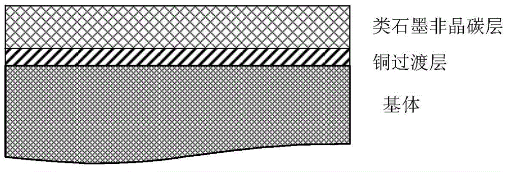
[0032] In this embodiment, the substrate material is silicon and stainless steel, and the conductive coating on the surface of the substrate consists of a copper transition layer on the surface of the substrate and a graphite-like amorphous carbon layer on the surface of the copper transition layer.
[0033] The preparation method of this conductive coating comprises the steps:
[0034] (1) Place the silicon substrate and the stainless steel substrate on the workpiece bracket of the magnetron sputtering coating chamber respectively, and vacuumize the chamber until the air pressure drops to 5×10 -3 Below Pa, argon gas is introduced to keep the cavity pressure at 1.2Pa, and a negative bias voltage of 500V is applied to the substrate at the same time, and the substrate is cleaned by glow plasma for 20 minutes;
[0035] (2) Introduce argon gas into the chamber so that the chamber pressure is 0.4Pa, the negative bias voltage of the substrate is 100V, and the metal copper is used as...
Embodiment 2
[0072] In this embodiment, the substrate material is silicon and stainless steel, and the conductive coating on the surface of the substrate consists of a copper transition layer on the surface of the substrate and a graphite-like amorphous carbon layer on the surface of the copper transition layer.
[0073] The preparation method of this conductive coating comprises the steps:
[0074] (1) Place the substrate on the workpiece bracket of the magnetron sputtering coating chamber, and vacuum the chamber until the air pressure drops to 5×10 -3 Below Pa, argon gas is introduced to keep the cavity pressure at 1.2Pa, and a negative bias of -500V is applied to the substrate at the same time, and the substrate is cleaned by glow plasma for 20 minutes;
[0075] (2) Introduce argon gas into the cavity, make the cavity pressure at 0.4Pa, keep the negative bias voltage of the substrate at 200V, use metal copper as the target material, turn on the DC magnetron sputtering source, and adjust...
PUM
| Property | Measurement | Unit |
|---|---|---|
| thickness | aaaaa | aaaaa |
| thickness | aaaaa | aaaaa |
| electrical resistivity | aaaaa | aaaaa |
Abstract
Description
Claims
Application Information


