A kind of anti-potential induced decay solar cell and preparation method thereof

A technology of potential-induced attenuation and solar cells, which is applied in the field of solar cells, can solve the problems of poor anti-potential-induced attenuation performance of batteries, unsatisfactory anti-potential-induced attenuation performance of batteries, and low refractive index, so as to improve battery conversion efficiency and increase Effect of resistance to potential induced decay performance

Active Publication Date: 2018-01-26
GUANGDONG AIKO SOLAR ENERGY TECH CO LTD +1
View PDF7 Cites 0 Cited by
  • Summary
  • Abstract
  • Description
  • Claims
  • Application Information

AI Technical Summary

Problems solved by technology

It can cause the power of a component to attenuate by more than 50%, thus affecting the power output of the entire power station
[0003] The reason for the potential-induced attenuation is mainly due to the migration of sodium ions in the packaging material of the battery module - glass and the upper surface layer and the lower surface layer under the action of high voltage: the sodium ions inside the glass migrate towards the solar cell, destroying the battery. p-n junction, resulting in attenuation of power
At present, the hot spot of anti-potential-induced decay technology is silicon oxide / silicon nitride laminated composite film technology. However, in the existing silicon oxide / silicon nitride laminated composite film, the refractive index of silicon oxide layer and silicon nitride layer are the same. lower
Thick silicon oxide and silicon nitride layers with low refractive index make the battery less resistant to potential-induced decay
[0004] There are also silicon dioxide films with a refractive index higher than 2.0 in the prior art. However, the optical matching between the silicon dioxide layer and other anti-reflection films is not very good, and the effect of blocking sodium ions is not ideal. Induced decay performance is not very ideal

Method used


Image

  • A kind of anti-potential induced decay solar cell and preparation method thereof
  • A kind of anti-potential induced decay solar cell and preparation method thereof

Examples


preparation example Construction

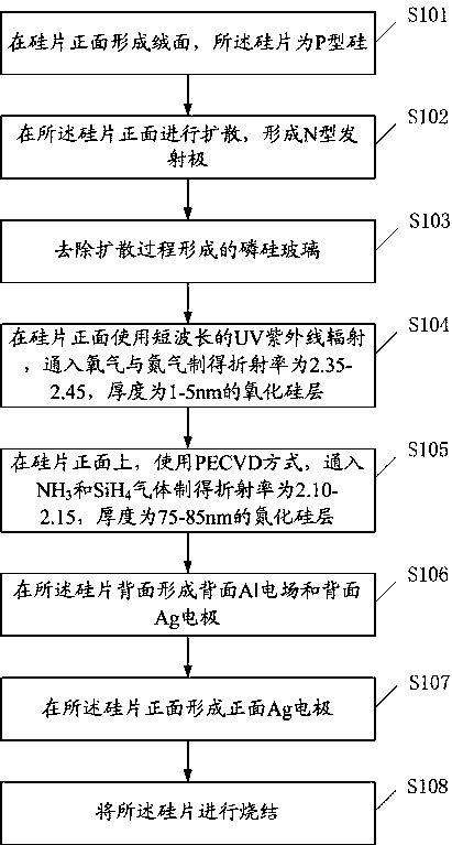
[0049] Correspondingly, see figure 2 , the invention provides a method for preparing a solar cell resistant to potential-induced decay, comprising:

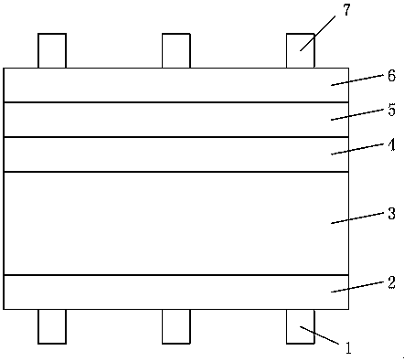
[0050] S101, forming a textured surface on the front surface of the silicon wafer, where the silicon wafer is P-type silicon.

[0051] The textured surface of the silicon chip adopts HF and / or HNO 3 solution to form an ideal suede structure and reduce reflectivity.

[0052] S102, performing diffusion on the front surface of the silicon wafer to form an N-type emitter.

[0053] The N-type emitter can be formed by methods such as thermal diffusion or ion implantation, wherein the diffusion of the silicon wafer is preferably made of phosphorus oxychloride.

[0054] S103, removing the phosphosilicate glass formed in the diffusion process.

[0055] Removing the phosphosilicate glass is beneficial to ensure the photoelectric conversion efficiency of the battery.

[0056] S104, using short-wavelength UV ultraviolet radiation on th...

Embodiment 1

[0067] Forming a suede surface on the front side of the silicon wafer, the silicon wafer is P-type silicon;

[0068] Diffusion is performed on the front side of the silicon wafer to form an N-type emitter;

[0069] Removal of phosphosilicate glass formed by the diffusion process;

[0070] Use short-wavelength UV ultraviolet radiation on the front of the silicon wafer, and pass oxygen and nitrogen to prepare a silicon oxide layer with a refractive index of 2.35 and a thickness of 1nm. The reaction temperature is 50°C, the oxygen flow rate is 15L / min, and the nitrogen flow rate is 10L / min, deposition time 8s;

[0071] On the front side of the silicon wafer, using the PECVD method, first pass the reaction gas NH 3 3.5 slm and SiH 4 900 sccm, the reaction time is 200 s to form the first layer of silicon nitride film; then, change the NH 3 and SiH 4 flow, the NH 3 Flow rate is set to 4.5slm, SiH 4 The flow rate is set to 500 sccm, the reaction time is 390s, and the second ...

Embodiment 2

[0076] Forming a suede surface on the front side of the silicon wafer, the silicon wafer is P-type silicon;

[0077] Diffusion is performed on the front side of the silicon wafer to form an N-type emitter;

[0078] Removal of phosphosilicate glass formed by the diffusion process;

[0079] Use short-wavelength UV ultraviolet radiation on the front of the silicon wafer, and pass oxygen and nitrogen to prepare a silicon oxide layer with a refractive index of 2.37 and a thickness of 2nm. The reaction temperature is 52°C, the oxygen flow rate is 17L / min, and the nitrogen flow rate is 12L / min, deposition time 9s;

[0080] On the front side of the silicon wafer, using the PECVD method, first pass the reaction gas NH 3 3.7 slm and SiH 4 950 sccm, reaction time 205 s to form the first layer of silicon nitride film; then, change the NH 3 and SiH 4 flow, the NH 3 Flow rate is set to 4.8slm, SiH 4The flow rate is set to 600 sccm, the reaction time is 400s, and the second layer of...


PUM

PropertyMeasurementUnit
thicknessaaaaaaaaaa
thicknessaaaaaaaaaa
thicknessaaaaaaaaaa

Abstract

The invention discloses a solar cell resisting potential-induced degradation. The solar cell comprises a back surface Ag electrode, a back surface Al electric field, P-type silicon, an N-type emitting electrode, a silicon oxide layer, a silicon nitride layer and a front surface Ag electrode which are arranged from the bottom to the top in turn. The refractive index of the silicon oxide layer is 2.35-2.45 and thickness is 1-5nm. The refractive index of the silicon nitride layer is 2.10-2.15 and thickness is 75-85nm. With application of the solar cell, potential-induced degradation resisting performance of the cell is greatly enhanced by the superposition structure of high-refractive-index silicon oxide-high-refractive-index silicon nitride under the premise of enhancing cell conversion efficiency.

Description

technical field [0001] The invention relates to the technical field of solar cells, in particular to a solar cell capable of resisting potential-induced attenuation and a preparation method thereof. Background technique [0002] Potential Induced Degradation PID (Potential Induced Degradation) or HVS (High Voltage Stress) refers to the phenomenon of output power attenuation caused by leakage current caused by high temperature and high humidity environment of photovoltaic power generation system under high voltage bias. The actual use of some power stations shows that the system voltage seems to have a continuous "potential-induced attenuation" effect on crystalline silicon battery components, and the leakage current caused by the circuit formed by the packaging material (usually the upper surface of EVA and glass) to the component frame, identified as the main cause of the above effects. It can cause the power of a component to attenuate by more than 50%, thus affecting the...

Claims


Application Information

Patent Timeline
Patent Type & Authority Patents(China)
IPC IPC(8): H01L31/0216H01L31/054H01L31/18
CPCH01L31/02168H01L31/02363H01L31/1804Y02E10/52Y02E10/547Y02P70/50
Inventor 秦崇德方结彬石强黄玉平何达能
Owner GUANGDONG AIKO SOLAR ENERGY TECH CO LTD
Why Eureka
Try Eureka