High-thermal-conductivity silicon nitride ceramic copper-clad plate and manufacturing method thereof

A technology of silicon nitride ceramics with high thermal conductivity, applied in semiconductor/solid-state device manufacturing, semiconductor devices, semiconductor/solid-state device components, etc., can solve the problems affecting the reliability of power modules, low bending strength and fracture toughness, and easy cracking and other problems, to achieve the effect of strong temperature shock resistance, improved strength and impact resistance, and less voids

Active Publication Date: 2015-03-11
HEBEI SINOPACK ELECTRONICS TECH
View PDF2 Cites 27 Cited by
  • Summary
  • Abstract
  • Description
  • Claims
  • Application Information

AI Technical Summary

Problems solved by technology

However, whether it is alumina or aluminum nitride ceramic substrate, its flexural strength and fracture toughness are relatively low,...

Method used


Image

  • High-thermal-conductivity silicon nitride ceramic copper-clad plate and manufacturing method thereof
  • High-thermal-conductivity silicon nitride ceramic copper-clad plate and manufacturing method thereof
  • High-thermal-conductivity silicon nitride ceramic copper-clad plate and manufacturing method thereof

Examples


preparation example Construction

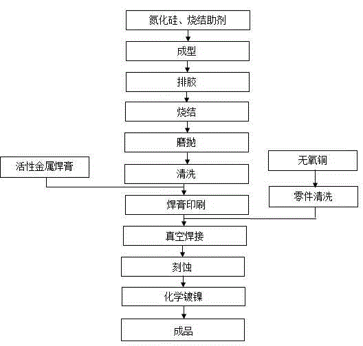
[0022] Such as image 3 As shown, the method for preparing a high thermal conductivity silicon nitride ceramic copper clad laminate of the present invention includes the following steps:

[0023] (1) Mixing ceramic powder and sintering aids into porcelain powder, the weight content of the ceramic powder is 90%-96%, and the sintering aids are yttrium oxide, aluminum oxide, magnesium oxide, and calcium oxide. One or more of the components, the weight content of which is 4%-10%, the thin-plate silicon nitride ceramic body is prepared by dry pressing, casting or gel injection molding;

[0024] (2) The thin-plate silicon nitride ceramic body is sintered under atmospheric pressure to prepare high thermal conductivity silicon nitride ceramic, and the ceramic surface is ground and polished to obtain a high thermal conductivity silicon nitride ceramic substrate;

[0025] (3) Stir and mix the metal Ag, Cu, Ti or Ag, Cu, Zr powders and then add an organic binder and stir to prepare Ti-Ag-Cu or...

Embodiment 1

[0030] Example 1: The above steps are the same, the weight content of the ceramic powder component is 90%. The sintering aid component is one or more of yttrium oxide, aluminum oxide, magnesium oxide, and calcium oxide, and its component weight content is 10% .

Embodiment 2

[0031] Example 2: The above steps are the same, the weight content of ceramic powder components is 96%. The sintering aid component is one or more of yttrium oxide, aluminum oxide, magnesium oxide, and calcium oxide, and its component weight content is 4% .


PUM


Abstract

The invention discloses a high-thermal-conductivity silicon nitride ceramic copper-clad plate and a manufacturing method thereof and relates to the field of the copper-clad plate manufacturing technology. The high-thermal-conductivity silicon nitride ceramic copper-clad plate comprises a high-thermal-conductivity silicon nitride ceramic substrate and oxygen-free copper layers; the upper and lower surfaces of the high-thermal-conductivity silicon nitride ceramic substrate are respectively welded with the oxygen-free copper layers; and the welding is a high-temperature welding in a vacuum brazing furnace by using an active metal welding paste. The bending strength of the high-strength and high-thermal-conductivity silicon nitride ceramic substrate is 2-3 times that of an aluminum nitride ceramic substrate, and the cladding of the high-thermal-conductivity silicon nitride ceramic substrate and a thick copper substrate can be realized; the thermal conductivity is 3-4 times that of the aluminum nitride ceramic substrate, so that the heat dissipation performance of the substrate can be improved greatly; compared with a direct copper-cladding process, the active copper-welding process has higher interface bonding strength, less cavities and higher reliability. Therefore, the high-thermal-conductivity silicon nitride ceramic copper-clad plate has the features of high strength, high conductivity and high reliability.

Description

Technical field [0001] The invention belongs to the technical field of copper clad laminate manufacturing, and specifically relates to a high thermal conductivity silicon nitride ceramic copper clad laminate and a preparation method thereof. Background technique [0002] Insulated gate bipolar transistor (IGBT) is the most important high-power device in the field of power electronics, and it is widely used in electric vehicles, electric locomotives and other fields. Ceramic copper clad laminate is a composite metal ceramic substrate formed by directly bonding high-conductivity oxygen-free copper to the ceramic surface at high temperature. It has the high thermal conductivity, high electrical insulation, high mechanical strength, low expansion, etc. of ceramics. It also has the high conductivity of oxygen-free copper metal and excellent soldering performance, and can etch various patterns like PCB circuit boards. It is an indispensable key basic material for power module packaging...

Claims


Application Information

Patent Timeline
IPC IPC(8): H01L23/15H01L23/373H01L21/48
Inventor 赵东亮刘志平刘圣迁郝宏坤杨哲
Owner HEBEI SINOPACK ELECTRONICS TECH
Why Eureka
Try Eureka