

a gese 2 Nanocrystal and its preparation method and application
A nanocrystal, temperature reaction technology, applied in nanotechnology, nanotechnology, nanotechnology for materials and surface science, etc., can solve the problems of harsh reaction conditions, high temperature, high energy consumption, and achieve low reaction temperature and time. Short, easy-to-use effects
- Summary
- Abstract
- Description
- Claims
- Application Information
AI Technical Summary
Problems solved by technology
Method used
Image

Examples
Embodiment 1
[0033] At room temperature, in a clean and dry 100 mL three-necked flask, add 0.290 g GeI 4 , 0.062 g selenourea and 15 mL oleylamine. Then, the above mixture was added to 5 o Cmin -1 heating rate to 280 o C and kept at this temperature for 60 min. Naturally cooled to room temperature after the reaction was finished, an orange-yellow precipitate was obtained, which was separated by centrifugation and washed 4-5 times with n-heptane and absolute ethanol, 40 o The product was dried under vacuum at C for analysis and characterization.
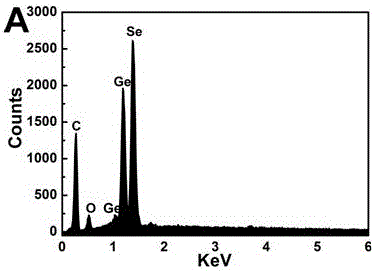
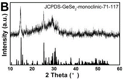
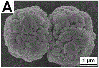
[0034] The product was analyzed by XRD, EDS, SEM, HRTEM and mapping test (element surface distribution diagram) (Fig. 1, Fig. 2, Fig. 3), and it was proved that the composition of the obtained product only contained two elements, Ge and Se, and they were evenly distributed in the The GeSe 2 in semiconductor materials. XRD analysis ( Figure 1B ) shows that the resulting product is pure GeSe 2 Nanocrystals have a monoclinic phase structure...
Embodiment 2
[0036] The monoclinic GeSe prepared in Example 1 of the present invention 2 The nanocrystals are modified on the ITO electrode, and the photoelectrochemical (PEC) measurement is carried out. The specific process is as follows:
[0037] Photoelectric test sample preparation: Weigh the sample to be tested GeSe 2 0.004 g was ultrasonically dispersed in a mixed solution of 2 mL of ethanol and water, and 10 μL of the above-mentioned dispersion was evenly dropped on the ITO electrode with a pipette gun, and it was used for testing after it was naturally dried.
[0038] Photoelectric tests were performed on a Zahner photoelectrochemical workstation. Three-electrode working system: GeSe 2 The modified ITO electrode was used as the working electrode, the Ag / AgCl was used as the reference electrode, and the platinum wire was used as the counter electrode. Electrolyte is 0.1 M PBS buffer solution (pH=7.4, 0.1 M PBS is NaH 2 PO 4 and Na 2 HPO 4 mixed preparation), adding 0.300 g o...
PUM
| Property | Measurement | Unit |
|---|---|---|
| diameter | aaaaa | aaaaa |
| diameter | aaaaa | aaaaa |
| width | aaaaa | aaaaa |
Abstract
Description
Claims
Application Information