Method for improving open-circuit voltage of amorphous silicon tandem solar cell

A solar cell and open-circuit voltage technology, applied in circuits, photovoltaic power generation, electrical components, etc., can solve the problem of insignificant increase in Voc

Inactive Publication Date: 2015-04-01
HANGZHOU AMPLESUN SOLAR TECH
View PDF3 Cites 0 Cited by
  • Summary
  • Abstract
  • Description
  • Claims
  • Application Information

AI Technical Summary

Problems solved by technology

[0005] However, the use of microcrystalline N-type materials or heavily doped N-type amorphous silicon materials does not significantly improve Voc

Method used


Image

  • Method for improving open-circuit voltage of amorphous silicon tandem solar cell
  • Method for improving open-circuit voltage of amorphous silicon tandem solar cell
  • Method for improving open-circuit voltage of amorphous silicon tandem solar cell

Examples


Embodiment 1( comparative Embodiment )

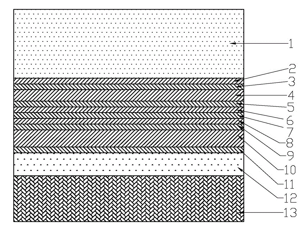
[0053] 1) With a transparent conductive glass (F-SnO2) with a tin oxide film thickness of 700nm as the substrate, a 10nm top-cell amorphous silicon P-type layer and a 10nm top-cell amorphous silicon P-type layer were sequentially deposited by 13.56MHz plasma chemical vapor deposition Buffer layer, 50nm top cell amorphous silicon I layer, 10nm top cell microcrystalline silicon N-type layer, 3nm bottom cell amorphous silicon P1 layer, 10nm bottom cell amorphous silicon P2 layer, 10nm amorphous silicon buffer Layer, 150nm bottom cell amorphous silicon I layer, 10nm bottom cell amorphous silicon N-type layer;

[0054] Among them, when depositing the microcrystalline silicon N-type layer of the top cell, the flow rate of phosphine is 200 sccm, the flow rate of hydrogen gas is 10 slm, and the flow rate of silane is 400 sccm; the deposition pressure of the microcrystalline N-type layer is 220 Pa, and the deposition power is 1.3 kW. When depositing the bottom cell amorphous silicon P1...

Embodiment 2

[0059] 1) Use transparent conductive glass (F-SnO2) with a tin oxide film thickness of 700nm as the substrate 1, and use 13.56MHZ plasma chemical vapor deposition to sequentially deposit a 10nm top cell amorphous silicon P-type layer, and a 10nm top cell amorphous silicon layer. Silicon buffer layer, 50nm top cell amorphous silicon I layer, 10nm top cell microcrystalline silicon N-type layer, 3nm bottom cell amorphous silicon P1 layer, 3nm bottom cell amorphous silicon P2 layer, 10nm bottom cell non-crystalline silicon Crystalline silicon P3 layer, 10nm amorphous silicon buffer layer, 150nm bottom cell amorphous silicon I layer, 10nm bottom cell amorphous silicon N-type layer;

[0060] Wherein, when depositing the microcrystalline silicon N-type layer 5 of the top cell, the pH 3 (phosphine) flow is 200sccm, H 2 (Hydrogen) with a flow rate of 10slm, SiH 4 The flow rate of (silane) is 400 sccm; the deposition pressure of the microcrystalline N-type layer is 220 Pa, and the dep...

Embodiment 3

[0065] 1) Use transparent conductive glass (F-SnO2) with a tin oxide film thickness of 700nm as the substrate 1, and use 13.56MHZ plasma chemical vapor deposition to sequentially deposit a 10nm amorphous silicon P-type layer for the top cell, and a 10nm amorphous silicon layer for the top cell Silicon buffer layer, 50nm top cell amorphous silicon I layer, 10nm top cell microcrystalline silicon N-type layer, 3nm bottom cell amorphous silicon P1 layer, 3nm bottom cell amorphous silicon P2 layer, 10nm bottom cell non-crystalline silicon Crystalline silicon P3 layer, 10nm amorphous silicon buffer layer, 150nm bottom cell amorphous silicon I layer, 10nm bottom cell amorphous silicon N-type layer;

[0066] Among them, when depositing the microcrystalline silicon N-type layer 5 of the top cell, the flow rate of phosphine is 200 sccm, the flow rate of hydrogen gas is 10 slm, and the flow rate of silane is 400 sccm; the deposition pressure of the microcrystalline N-type layer is 220 Pa,...


PUM


Abstract

The invention discloses a method for improving open-circuit voltage of an amorphous silicon tandem solar cell, and belongs to the technical field of solar cells. According to the method, a bottom cell P-type layer structure in a conventional amorphous silicon tandem cell is changed to a P-type three-layer structure including a bottom cell amorphous silicon layer P1, a bottom cell amorphous silicon layer P2 and a bottom cell amorphous silicon layer P3; and three layers of structures are amorphous silicon material layers doped with boron and carbon, and the carbon doping amount of the bottom cell amorphous silicon layer P1, the bottom cell amorphous silicon layer P2 and the bottom cell amorphous silicon layer P3 is sequentially increased. Interface contact between a bottom cell and a top cell is improved, and a built-in electric field is enhanced, so that open circuit of the amorphous silicon tandem cell is greatly increased, and meanwhile, the photoelectric conversion efficiency of the amorphous silicon tandem cell is improved. Compared with a conventional amorphous silicon tandem solar cell, the open-circuit voltage of the amorphous silicon tandem solar cell is improved by 10.5 V at most with adoption of the method.

Description

technical field [0001] The invention belongs to the field of amorphous silicon thin-film solar cells, in particular to the technology of amorphous silicon thin-film laminated solar cells. Background technique [0002] At present, there are two ways to improve the open circuit voltage of amorphous silicon laminated cells: 1. The N-type layer of the top cell uses microcrystalline silicon N-type material; 2. The N-type layer of the top cell uses heavily doped N-type amorphous silicon material. [0003] The N-type layer of the top cell is made of microcrystalline N-type layer material, which reduces the series resistance of the battery, and can well improve the current flow problem on the NP reverse junction inside the tandem solar cell, so that the NP reverse junction inside the battery forms a good Ohmic contact is also beneficial to reduce solid-phase interdiffusion, improve stability, and increase Voc and Isc of the battery. [0004] The N-type layer of the top cell is made...

Claims


Application Information

Patent Timeline
Patent Type & Authority Applications(China)
IPC IPC(8): H01L31/20H01L31/0352H01L31/0288
CPCH01L31/0288H01L31/0352H01L31/03762H01L31/202Y02E10/548Y02P70/50
Inventor 李媛吴兴坤周丽萍刘金智
Owner HANGZHOU AMPLESUN SOLAR TECH
Why Eureka
Try Eureka