Laser grooving gate-buried electrode solar cell and method for preparing the same
A technology of solar cells and buried gate electrodes, which is applied in the field of solar cells, can solve the problems of unsatisfactory photoelectric conversion efficiency of solar cells, unsatisfactory passivation effect of solar cells, and low bonding strength between coating and substrate, so as to increase the passivation of front and rear surfaces The effect of improving the conversion efficiency of the battery and reducing the pollution of surface metal impurities
- Summary
- Abstract
- Description
- Claims
- Application Information
AI Technical Summary
Problems solved by technology
Method used
Image
Examples
preparation example Construction
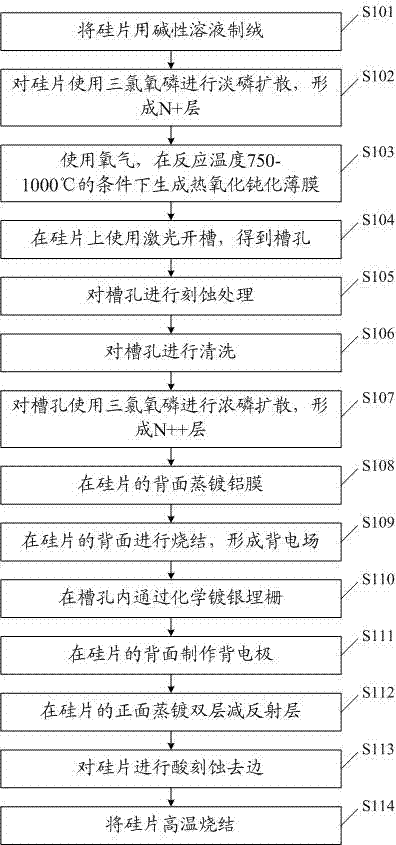
[0041] see figure 1 , the invention provides a method for preparing a solar cell with a laser-grooved buried gate electrode, comprising:
[0042] S101. Texturing the silicon wafer with an alkaline solution
[0043] Since the reaction between alkaline solution and silicon (Si) will form anisotropic corrosion, the present invention uses alkaline solution to make texture with the following advantages: use the anisotropic physical properties of the single crystal structure to participate in the reaction to form a uniform low reflection Ratio textured pyramid-like surface topography greatly reduces photon reflection and increases light absorption.
[0044] The existing method of making texture is acid texture, the disadvantage is that the reflectivity is high and the uniformity of the texture is poor.
[0045] Preferably, the alkaline solution is NaOH, Na 2 SiO 4 and IPA mixed solution, NaOH : Na 2 SiO 4 : IPA = 1: 1-2 : 1-2, the texturing temperature is 80-90℃.
[0046] I...
Embodiment 1
[0099] P-type silicon with NaOH, Na 2 SiO 4 and IPA mixed solution (NaOH : Na 2 SiO 4 : IPA = 1: 1 : 1) Carry out texturing at 80°C;
[0100] Phosphorus oxychloride is used for light phosphorus diffusion on silicon wafers to form an N+ layer;
[0101] Use oxygen with a purity of 99% to form a thermal oxidation passivation film with a thickness of 15nm at a reaction temperature of 750°C;
[0102] Use Nd:YAG laser for slotting, the wavelength of the laser is 532nm, to obtain rectangular slots with a width of 25nm, a depth of 35um, and a spacing of 1mm;
[0103] Use a mixed solution of hydrofluoric acid and nitric acid (hydrofluoric acid: nitric acid = 1:2) to etch the slot holes at 25°C;
[0104] The wells are cleaned, including with SPM solution (H 2 SiO 4 :H 2 o 2 =3:1) for the first cleaning at a temperature of 100°C, with DHF solution (HF: H 2 O=1:90) at room temperature for the second wash with APM solution (NH 4 OH:H 2 o 2 :H 2 O=1: 1:5) for the third clean...
Embodiment 2
[0114] P-type silicon with NaOH, Na 2 SiO 4 and IPA mixed solution (NaOH : Na 2 SiO 4 : IPA = 1: 1.5 : 1.5) Carry out texturing at 85°C;
[0115] Phosphorus oxychloride is used for light phosphorus diffusion on silicon wafers to form an N+ layer;
[0116] Use oxygen with a purity of 99.9995% to form a thermal oxidation passivation film with a thickness of 20nm at a reaction temperature of 850°C;
[0117] Use Nd:YAG laser for slotting, the wavelength of the laser is 532nm, and a rectangular slot with a width of 30nm, a depth of 40um, and a spacing of 1.5mm is obtained;
[0118] Use a mixed solution of hydrofluoric acid and nitric acid (hydrofluoric acid: nitric acid = 1:2.5) to etch the slot holes at 30°C;
[0119] The wells are cleaned, including with SPM solution (H 2 SiO 4 :H 2 o 2 =4:1) for the first cleaning at a temperature of 110°C, with DHF solution (HF: H 2 O=1:100) at room temperature for the second wash with APM solution (NH 4 OH:H 2 o 2 :H 2 O=1: 1:4...
PUM
 Abstract
Description
Claims
Application Information

