SnO2 porous structure perovskite photovoltaic cell and preparation method thereof
A porous structure, photovoltaic cell technology, applied in photovoltaic power generation, circuits, electrical components and other directions, can solve the problems of long-term stability, not suitable for industrial applications, reduce battery stability and other problems, achieve large commercial application prospects, good Photoelectric conversion efficiency and stable performance, low cost effect
- Summary
- Abstract
- Description
- Claims
- Application Information
AI Technical Summary
Problems solved by technology
Method used
Image
Examples
Embodiment 1
[0048] 1) Wash. In the test, the FTO conductive glass substrate should be cleaned and dried first. Clean the FTO conductive glass of appropriate size with detergent first, and then rinse it with deionized water. Then use deionized water, acetone, ethanol to clean ultrasonically, and finally blow dry with nitrogen for later use.
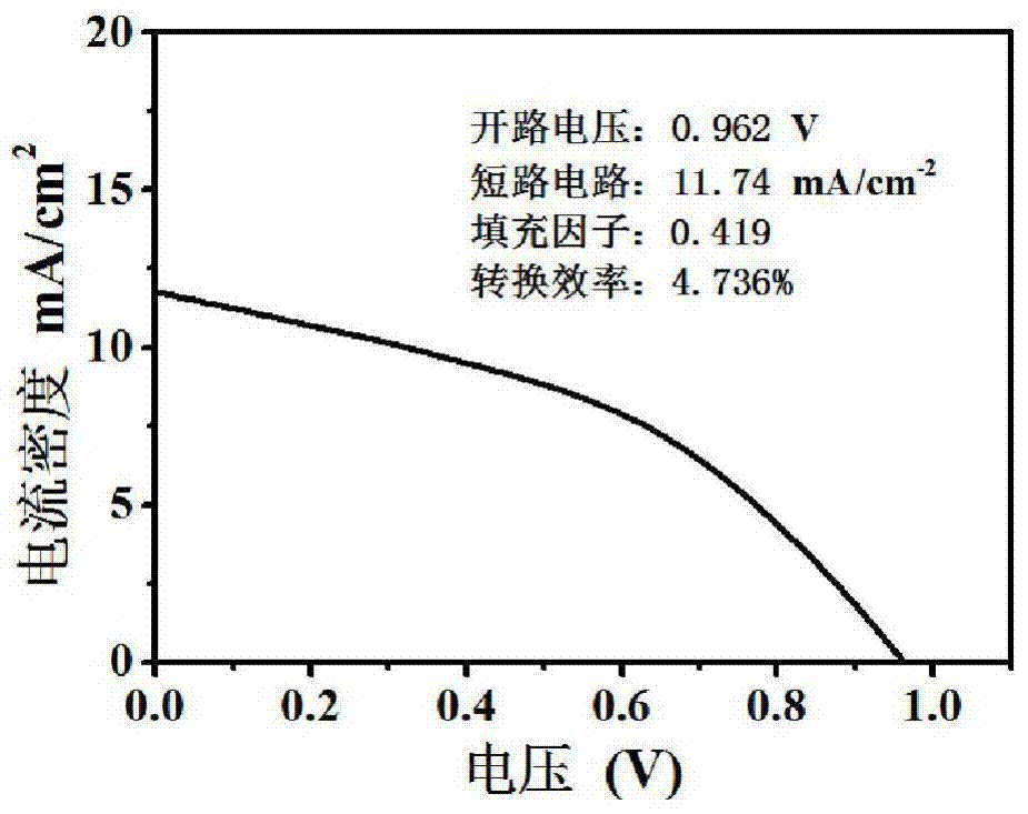
[0049] 2) Perovskite CH 3 NH 3 PB 3 Absorbing layer preparation. Configuration of perovskite solution: 1M PbCl 2 Dissolve in dimethylformamide and stir at 60°C for 24 hours. Then use the homogenizer to mix the PbCl 2 The solution was spin-coated on the FTO conductive glass substrate, and then annealed at 70°C for 30 minutes. Spin coated with PbCl 2 The sample was placed in 10 mg / L CH 3 NH 3 Immerse in isopropanol solution for 5 minutes; finally rinse the sample with isopropanol, blow dry with nitrogen, and anneal at 70°C for 30 minutes.
[0050] 3) Preparation of hole transport layer. perovskite CH with a homogenizer 3 NH 3 PB 3 A laye...
Embodiment 2
[0054] (1) cleaning. With embodiment 1.
[0055] (2) SnO 2 Dense layer preparation. 0.1 M SnCl 2 2H 2 O ethanol solution was stirred for 30 minutes, and then the precursor solution was spin-coated on the cleaned FTO conductive glass with a homogenizer; the spin-coated SnO 2 The solution of the FTO conductive glass was annealed at 200 °C for 30 min.
[0056] (3) Perovskite CH 3 NH 3 PB 3 Absorbing layer preparation. With embodiment 1.
[0057] (4) Preparation of hole transport layer. With embodiment 1.
[0058] (5) Electrode preparation. Same implementation benefit 1.
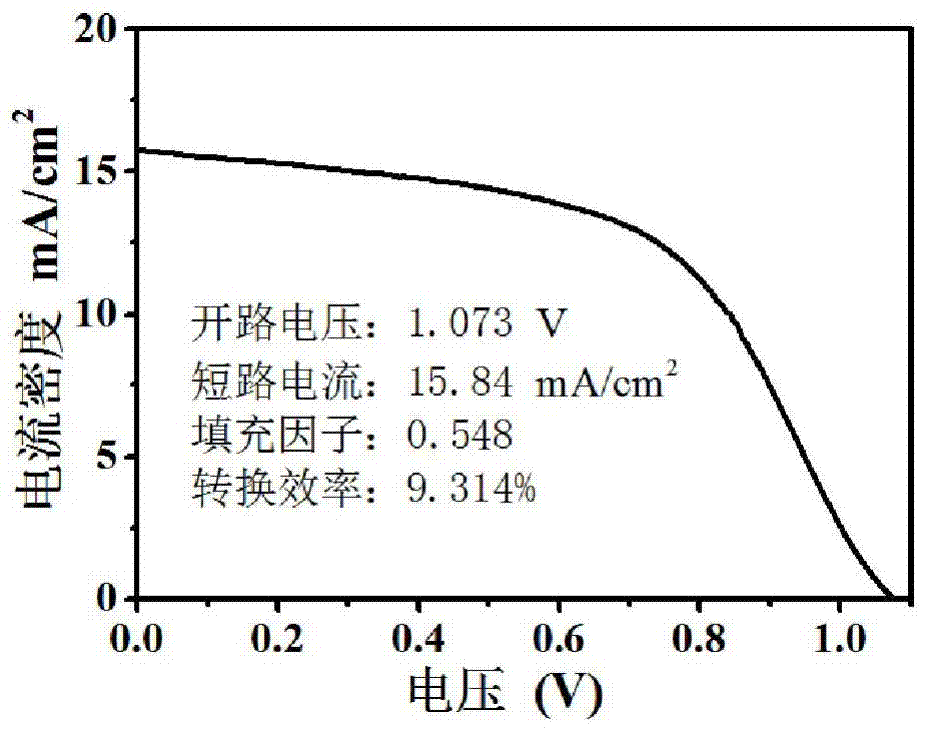
[0059] (6) Test, same as Example 1. The obtained photoelectric conversion efficiency parameters are, open circuit voltage 1.073 V, short circuit current density 15.84 mA / cm 2 , fill factor 0.548, conversion efficiency 9.314%.
Embodiment 3
[0061] (1) cleaning. With embodiment 1.
[0062] (2) SnO 2 Dense layer preparation. With embodiment 2.
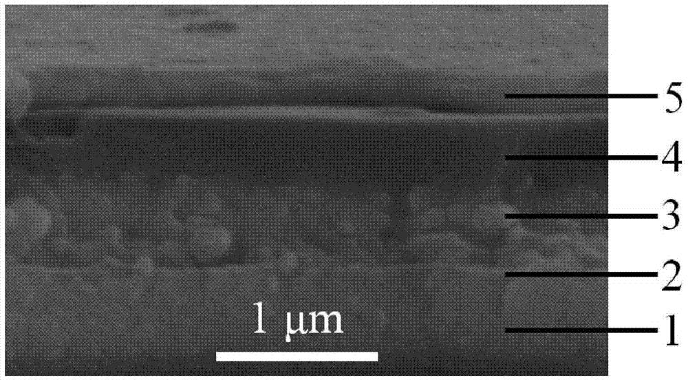
[0063] (3) SnO 2 Porous layer preparation. 90 mg SnCl 2 2H 2 O was dissolved in 4 mL ethanol solution and stirred for 30 min to obtain SnO 2 Sol; add 0.3g polyethylene glycol with a molecular weight of 20000 and 100 μL Triton x-100 to the above sol, and stir thoroughly for more than 12 hours to obtain SnO 2 Precursor;
[0064] (4) Mix SnO with a homogenizer 2 Precursor spin-coated on annealed SnO 2 on the dense layer;
[0065] (5) Rapidly anneal the product obtained in step 4 at 500 degrees Celsius for 60 seconds.
[0066] (6) Perovskite CH 3 NH 3 PB 3 Absorbing layer preparation. With embodiment 1.
[0067] (7) Preparation of hole transport layer. With embodiment 1.
[0068] (8) Electrode preparation. Same implementation benefit 1.
[0069] (9) Test, same as Example 1. The obtained photoelectric conversion efficiency parameters are, open circuit volta...
PUM
 Abstract
Description
Claims
Application Information


