Organic light-emitting device packaging structure and packaging method thereof

An electroluminescent device and packaging structure technology, applied in the direction of electric solid devices, electrical components, semiconductor devices, etc., can solve the problems of loss of absorption capacity of desiccant, decrease of device life, easy to produce cracks, etc., to achieve good step coverage and The effect of large area thickness uniformity, small influence and strong adhesion

Inactive Publication Date: 2015-04-15
OCEANS KING LIGHTING SCI&TECH CO LTD +2
View PDF0 Cites 0 Cited by
  • Summary
  • Abstract
  • Description
  • Claims
  • Application Information

AI Technical Summary

Problems solved by technology

As the desiccant in the device absorbs a large amount of oxygen and water vapor, the desiccant loses its absorption capacity in a short period of time, resulting in the gradual accumulation of oxygen and water vapor in the device, which significantly reduces the life of the device; the glass cover usually used Or the metal cover plate is a brittle material, which is prone to cracks, and the device will appear very thick after packaging, which is not suitable for flexible devices

Method used


Image

  • Organic light-emitting device packaging structure and packaging method thereof
  • Organic light-emitting device packaging structure and packaging method thereof
  • Organic light-emitting device packaging structure and packaging method thereof

Examples


Embodiment 1

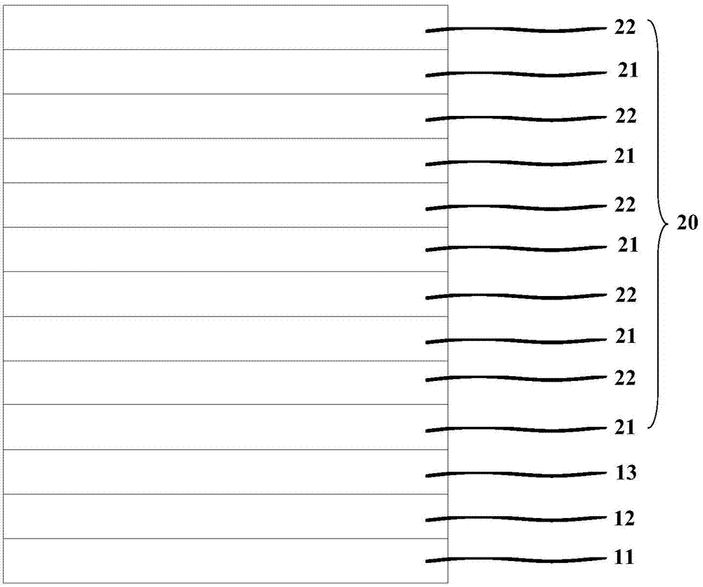
[0058] figure 1 It is a schematic diagram of the packaging structure of the organic electroluminescent device in Example 1; as figure 1 Shown, the encapsulation structure of this organic electroluminescent device comprises ITO glass substrate (11), organic luminescence functional layer (12), cathode (13) and thin film encapsulation layer (20); Thin film encapsulation layer (20) comprises 5 by A packaging unit composed of a germanium carbonitride film layer (21) and an inorganic barrier layer (22).

[0059] A method for encapsulating an organic electroluminescent device, comprising the steps of:

[0060] (1) Pre-treatment of ITO glass substrate (11): First, clean the ITO glass with acetone, ethanol, deionized water, and ethanol in sequence, all of which are cleaned with an ultrasonic cleaner. dry, oven dry stand-by; then surface activation treatment is carried out to the cleaned ITO glass, to increase the oxygen content of the conductive surface layer, improve the work functi...

Embodiment 2

[0076] A method for encapsulating an organic electroluminescent device, comprising the steps of:

[0077] (1), (2), (3) are the same as embodiment 1;

[0078] (4) Preparation of thin film encapsulation layer:

[0079] a) Preparation of germanium carbonitride film layer: the germanium carbonitride film layer was prepared on the surface of the cathode by plasma enhanced chemical vapor deposition (PECVD), the working pressure was 10Pa, the deposition temperature was 30°C, and the radio frequency power was 0.1W / cm 2 ; The gas sources used in the process of depositing the germanium carbonitride layer are methylgermane (MMG), ammonia (NH 3 ) and hydrogen (H 2 ), hydrogen (H 2 ) flow rate is 205 sccm, methylgermane (MMG) flow rate is 8 sccm, ammonia (NH 3 ) / methylgermane (MMG) ratio range is 24, germanium carbonitride film thickness is 140nm;

[0080] b) Preparation of inorganic barrier layer: Atomic layer deposition (ALD) was used to prepare an inorganic barrier layer on the ...

Embodiment 3

[0085] A method for encapsulating an organic electroluminescent device, comprising the steps of:

[0086] (1), (2), (3) are the same as embodiment 1;

[0087] (4) Preparation of thin film encapsulation layer:

[0088] a) Preparation of germanium carbonitride film layer: the germanium carbonitride film layer was prepared on the cathode surface by plasma enhanced chemical vapor deposition (PECVD), the working pressure was 50Pa, the deposition temperature was 50°C, and the radio frequency power was 0.5W / cm 2 ; The gas sources used in the process of depositing the germanium carbonitride layer are methylgermane (MMG), ammonia (NH 3 ) and hydrogen (H 2 ), hydrogen (H 2 ) flow rate is 210 sccm, methylgermane (MMG) flow rate is 6 sccm, ammonia gas (NH 3 ) / methylgermane (MMG) ratio range is 21, germanium carbonitride film thickness is 140nm;

[0089] b) Preparation of inorganic barrier layer: Atomic layer deposition (ALD) was used to prepare an inorganic barrier layer on the sur...


PUM

PropertyMeasurementUnit
thicknessaaaaaaaaaa
thicknessaaaaaaaaaa
thicknessaaaaaaaaaa

Abstract

The invention discloses an organic light-emitting device packaging structure comprising an anode conductive substrate, and an organic light-emitting functional layer, a cathode and a film packaging layer which are sequentially stacked on the anode conductive substrate. The film packaging layer comprises a carbon nitride germanium film layer and an inorganic barrier layer which are sequentially stacked on the cathode, wherein the carbon nitride germanium film layer is made of a carbon nitride germanium compound, and the inorganic barrier layer is made of chlorine-doped titanium oxide, chlorine-doped zirconium oxide or chlorine-doped hafnium oxide. The film packaging layer of the packaging structure disclosed by the invention has very high density and effectively reduces the erosion of external oxygen, water vapor and other substances to organic compounds and electrodes in an organic light-emitting device. Therefore, devices are effectively protected, the service life of devices, flexible devices in particular, is increased, and the service life of devices is up to more than 14500 hours (T70@1000cd/m<2>). In the second aspect, the invention provided an organic light-emitting device packaging method.

Description

technical field [0001] The invention relates to the technical field of organic electroluminescent devices, in particular to a packaging structure and a packaging method for organic electroluminescent devices. Background technique [0002] Currently, organic electroluminescent devices (OLEDs) suffer from a short lifetime, which is mainly caused by the intrusion of oxygen and water vapor. On the one hand, oxygen is a quencher, which will significantly reduce the quantum efficiency of luminescence. At the same time, oxygen will oxidize the luminescent layer, and the carbonyl compound produced is also an effective quencher; on the other hand, the influence of water vapor is more obvious, it The main way of destruction is to make the organic compound in the device hydrolyze, and also react with the metal cathode, which greatly reduces its stability, resulting in device failure and reduced service life. Therefore, in order to effectively suppress the degradation and failure of or...

Claims


Application Information

Patent Timeline
Patent Type & Authority Applications(China)
IPC IPC(8): H01L51/50H01L51/52H01L51/54H01L51/56
CPCH10K50/8445H10K50/84H10K50/844H10K71/00
Inventor 周明杰钟铁涛王平张振华
Owner OCEANS KING LIGHTING SCI&TECH CO LTD
Why Eureka
Try Eureka