Encapsulation structure and encapsulation method of organic light emitting diode device
An electroluminescent device and packaging structure technology, which is applied in the direction of electric solid-state devices, electrical components, semiconductor devices, etc., can solve the problem that the barrier performance of plastic substrates cannot meet the requirements of OLED packaging, the life of flexible organic electroluminescent devices is short, and the device film There are many defects in the layer structure to achieve excellent packaging effect, which is beneficial to the life of the device and reduces the effect of erosion
- Summary
- Abstract
- Description
- Claims
- Application Information
AI Technical Summary
Problems solved by technology
Method used
Image


Examples
Embodiment 1
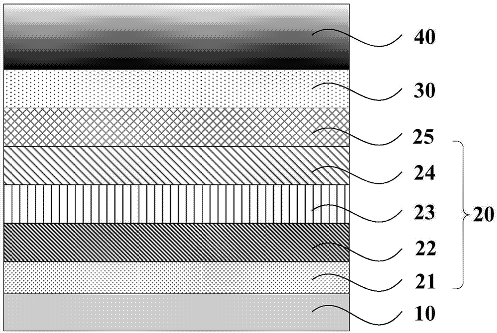
[0039] figure 1 It is a schematic diagram of the packaging structure of an organic electroluminescent device provided in this embodiment. Such as figure 1 As shown, the packaging structure of the organic electroluminescent device is sequentially stacked with a conductive glass substrate 10 , an organic light-emitting functional layer 20 , a metal cathode 30 and a packaging layer 40 . Wherein, the organic light-emitting functional layer 20 includes a hole injection layer 21 , a hole transport layer 22 , a light-emitting layer 23 , an electron transport layer 24 and an electron injection layer 25 stacked sequentially from bottom to top. figure 2 yes figure 1 Schematic diagram of the structure of the encapsulation layer, such as figure 2 As shown, the encapsulation layer 40 includes a germanium carbonitride layer 41 , a first barrier layer 42 and a second barrier layer 43 sequentially stacked on the metal cathode 30 . More specifically, the encapsulation layer 40 includes d...
Embodiment 2
[0055] A packaging structure of an organic electroluminescence device, which sequentially includes a conductive glass substrate, a hole injection layer, a hole transport layer, a light emitting layer, an electron transport layer, an electron injection layer, a metal cathode and a packaging layer from bottom to top. The encapsulation layer is composed of 4 layers of germanium carbonitride / Al 2 o 3 :Cl layer / ZrO 2 : Multilayer composite film structure composed of Cl layer. Its preparation method is as follows:
[0056] (1) Pre-treatment of ITO glass substrates: ITO glass substrates are cleaned with acetone, ethanol, deionized water, and ethanol, all of which are cleaned with an ultrasonic cleaner. The single washing is cleaned for 5 minutes, then blown dry with nitrogen, and dried in an oven Standby; the cleaned ITO glass also needs surface activation treatment to increase the oxygen content of the conductive surface layer and improve the work function of the conductive layer...
Embodiment 3
[0070] A packaging structure of an organic electroluminescence device, which sequentially includes a conductive glass substrate, a hole injection layer, a hole transport layer, a light emitting layer, an electron transport layer, an electron injection layer, a metal cathode and a packaging layer from bottom to top. The encapsulation layer is composed of 3 layers of germanium carbonitride / Ga 2 o 3 :Cl layer / HfO 2 : Multilayer composite film structure composed of Cl layer. Its preparation method is as follows:
[0071] (1) Pre-treatment of ITO glass substrates: ITO glass substrates are cleaned with acetone, ethanol, deionized water, and ethanol, all of which are cleaned with an ultrasonic cleaner. The single washing is cleaned for 5 minutes, then blown dry with nitrogen, and dried in an oven Standby; the cleaned ITO glass also needs surface activation treatment to increase the oxygen content of the conductive surface layer and improve the work function of the conductive layer...
PUM
| Property | Measurement | Unit |
|---|---|---|
| Thickness | aaaaa | aaaaa |
| Thickness | aaaaa | aaaaa |
| Deposition thickness | aaaaa | aaaaa |
Abstract
Description
Claims
Application Information
PatSnap Eureka turns technology decisions into work you can execute. Powered by our Innovation Knowledge Graph, it runs expert workflows across engineering, life sciences, materials and intellectual property. Get your review-ready output in minutes.


