Supercharge Your Innovation With Domain-Expert AI Agents!

Manufacturing technology for transistor

A preparation process and transistor technology, which is applied in semiconductor/solid-state device manufacturing, semiconductor devices, electrical components, etc., can solve problems such as limited technical effect, long crystallization time, and large grain roughness, so as to enhance flexibility and reduce Effects of roughness, process flexibility

Inactive Publication Date: 2015-04-22
KUNSHAN GO VISIONOX OPTO ELECTRONICS CO LTD
View PDF1 Cites 3 Cited by
  • Summary
  • Abstract
  • Description
  • Claims
  • Application Information

AI Technical Summary

Problems solved by technology

Among them, the uniformity of the crystal grains formed by excimer laser crystallization ELA is poor, and the roughness of the grains is large, and the surface protrusion height can reach 10~20nm, resulting in high leakage current. Although the HF and ozone water are used to clean alternately, Oxidize the Si surface and then use HF to remove the oxide layer to reduce the surface roughness of polysilicon, but its technical effect is very limited. At the same time, the excimer laser crystallization ELA is irradiated from the a-Si side, so this process must be in the gate Prior to metal deposition, resulting in less process flexibility
Another commonly used purification method, that is, low-temperature polysilicon LTPS formed by metal-induced crystallization, has the problem of metal ion contamination and high leakage current. At the same time, this method also has the disadvantages of long crystallization time and is not suitable for large-scale production. technical problem

Method used


Image

  • Manufacturing technology for transistor
  • Manufacturing technology for transistor
  • Manufacturing technology for transistor

Examples


preparation example Construction

[0033] The invention provides a transistor preparation process, specifically a low-leakage thin-film transistor low-temperature polysilicon preparation process. In any process after the deposition of amorphous silicon and before S / D heavy doping, the wavelength is 320nm~ The 550nm laser is irradiated from the side of the substrate 1 to melt and crystallize the amorphous silicon to form polysilicon, and then replace the conventional step of using a laser source to irradiate from the side of the substrate 1 with the film. And the present invention uses a laser source with a wavelength of 320nm~550nm instead of a 308nm laser source in the conventional preparation process.

[0034] The invention provides a preparation process of a transistor, comprising the following steps:

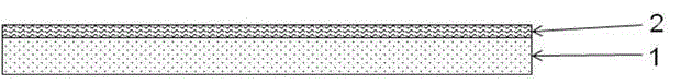
[0035] Step 1: If figure 1 As shown, the substrate 1 is selected, and a single-layer or double-layer buffer layer 2 is deposited on the substrate 1; then a layer of amorphous silicon layer 3 is deposited on ...

Embodiment 1

[0049] This embodiment provides a fabrication process for a transistor, including the following steps:

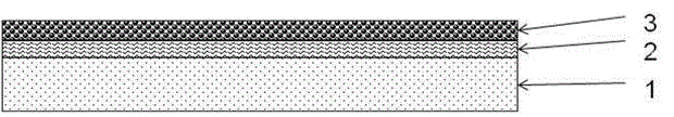
[0050] Step 1: If figure 1 As shown, the substrate 1 is selected, and a single-layer buffer layer 2 is deposited on the substrate 1; then a layer of amorphous silicon layer 3 is deposited on the buffer layer 2, and the amorphous silicon layer 3 is lightly doped amorphous silicon, such as figure 2 As shown, a-Si deposition is completed.

[0051] The substrate 1 may be a quartz substrate that transmits a laser wavelength of 320nm.

[0052] The material of the buffer layer 2 is Si 3 N 4 , with a thickness of 500nm. S

[0053] The thickness of the amorphous silicon layer 3 is 10nm, and the third main group is doped in the amorphous silicon layer 3, and its doping concentration is 1E10cm -2 , to increase the mobility of the amorphous silicon layer 3 .

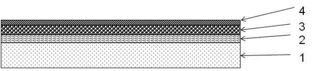
[0054] Step 2: If image 3 As shown, an insulating layer 4 with a thickness of 50 nm is deposited on the amorphous sil...

Embodiment 2

[0063] This embodiment provides a fabrication process for a transistor, including the following steps:

[0064] Step 1: If figure 1 As shown, the substrate 1 is selected, and a double-layer buffer layer 2 is deposited on the substrate 1; then a layer of amorphous silicon layer 3 is deposited on the buffer layer 2, and the amorphous silicon layer 3 is lightly doped amorphous silicon, such as figure 2 As shown, a-Si deposition is completed.

[0065] The substrate 1 may be an acrylic substrate that transmits 550nm laser light.

[0066] The material of the buffer layer 2 is SiO 2 , with a thickness of 300nm.

[0067] The thickness of the amorphous silicon layer 3 is 500nm, and the amorphous silicon layer 3 is doped with elements of the fifth main group (such as boron, phosphorus or arsenic) with a doping concentration of 1E12cm -2 , to increase the mobility of the amorphous silicon layer 3 .

[0068] Step 2: If Figure 4 As shown, a laser with a wavelength of 550nm is irrad...


PUM

PropertyMeasurementUnit
thicknessaaaaaaaaaa
thicknessaaaaaaaaaa
wavelengthaaaaaaaaaa

Abstract

The invention discloses a manufacturing technology for a transistor. The manufacturing technology comprises the steps that a laser radiation mode is adopted to carry out radiation from the side, without a film, of a substrate, and noncrystalline silicon is fused to form a polycrystalline silicon; a buffer layer, a noncrystalline silicon layer and an insulation layer are sequentially deposited on the substrate; photoetching is conducted on the noncrystalline silicon layer and the insulation layer to form a silicon island; a gate metal layer is deposited on the silicon island; a first interlayer dielectric layer is deposited, and contact holes are formed; heavy doping is conducted, and follow-up processes are conducted to form a source / drain electrode, a second interlayer dielectric layer, an indium tin oxide anode and a pixel limit layer. A covering layer is deposited on the noncrystalline silicon layer, and the roughness of the polycrystalline silicon is reduced after being crystallized. In addition, laser radiation crystallization can be executed in any step executed after noncrystalline silicon a-Si deposition and before S / D heavy doping, and the process flexibility is improved.

Description

technical field [0001] The invention relates to a preparation process of a transistor, in particular to a preparation process of low-temperature polysilicon for a low-leakage thin film transistor. Background technique [0002] The low-temperature polysilicon preparation process LTPS-TFT has higher mobility than the amorphous silicon preparation process a-Si-TFT, and is suitable for use in the drive circuit of the active matrix organic light-emitting diode panel AMOLED. Commonly used low-temperature polysilicon LTPS crystallization methods include excimer laser crystallization ELA and metal-induced crystallization. Among them, the uniformity of the crystal grains formed by excimer laser crystallization ELA is poor, and the roughness of the grains is large, and the surface protrusion height can reach 10~20nm, resulting in high leakage current. Although the HF and ozone water are used to clean alternately, Oxidize the Si surface and then use HF to remove the oxide layer to red...

Claims


Application Information

Patent Timeline
Patent Type & Authority Applications(China)
IPC IPC(8): H01L21/336H01L21/268
CPCH01L29/6675H01L21/268
Inventor 王迪
Owner KUNSHAN GO VISIONOX OPTO ELECTRONICS CO LTD
Features
  • R&D
  • Intellectual Property
  • Life Sciences
  • Materials
  • Tech Scout
  • Unparalleled Data Quality
  • Higher Quality Content
  • 60% Fewer Hallucinations
Learn More