High pressure resistant nitride semiconductor epitaxial structure and growing method thereof

A technology of nitride semiconductor and epitaxial structure, applied in semiconductor devices, semiconductor/solid-state device manufacturing, electrical components, etc., can solve the problem of reducing heterojunction channel mobility and two-dimensional electron gas carrier concentration, and reducing GaN crystal Quality, increase surface roughness and other issues, to achieve the effect of reducing epitaxial growth time, reducing production costs, and improving stress state

Inactive Publication Date: 2015-05-06
SUN YAT SEN UNIV
View PDF3 Cites 22 Cited by
  • Summary
  • Abstract
  • Description
  • Claims
  • Application Information

AI Technical Summary

Problems solved by technology

Josephine Selvaraj et al. studied the introduction of C impurities into the top layer of GaN under the channel layer under different growth conditions, which significantly improved the leakage current and breakdown voltage of the material [J. Selvaraj / Japanese Journal of Applied Physics 48(2009) 121002] , however, the C-doping of GaN on the top layer will greatly reduce the quality of GaN crystals and increase the surface roughness, thereby reducing the heterojunction channel mobility and the two-dimensional electron gas carrier concentration, thereby greatly deteriorating the device performance

Method used


Image

  • High pressure resistant nitride semiconductor epitaxial structure and growing method thereof
  • High pressure resistant nitride semiconductor epitaxial structure and growing method thereof
  • High pressure resistant nitride semiconductor epitaxial structure and growing method thereof

Examples


Embodiment 1

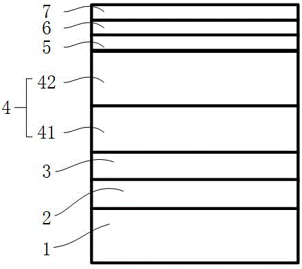
[0040] Such as figure 1 Shown is a schematic diagram of the epitaxial structure of this embodiment, including a substrate 1, a nucleation layer 2, an impurity filter layer 3, a compound nitride epitaxial buffer layer 4, an electron blocking layer 5, an undoped gallium nitride channel layer 6 and Heterojunction barrier layer 7. The composite nitride epitaxial buffer layer 4 includes a high-resistance aluminum-rich nitride stress buffer layer 41 and a high-resistance top layer gallium nitride buffer layer 42 on the high-resistance aluminum-rich nitride stress buffer layer 41 .

[0041] The growth method used in this solution is one of two methods: molecular beam epitaxy or metal organic chemical vapor deposition.

[0042] The above method for manufacturing a high withstand voltage nitride semiconductor epitaxial structure is as follows: figure 1 shown, including the following steps:

[0043] (1) A nucleation layer 2 is grown on the substrate 1 by molecular beam epitaxy or met...


PUM

PropertyMeasurementUnit
thicknessaaaaaaaaaa
thicknessaaaaaaaaaa
thicknessaaaaaaaaaa

Abstract

The invention relates to the technical field of epitaxial growth of semiconductor materials, and discloses a high pressure resistant nitride semiconductor epitaxial structure and a growing method thereof. The high pressure resistant nitride semiconductor epitaxial structure sequentially includes a substrate, a nucleating layer, an impurity filter layer, a complex nitride epitaxial buffer layer, an electron barrier layer, a non-doped gallium nitride channel layer and a heterojunction barrier layer from the bottom up; the complex nitride epitaxial buffer layer includes a high-resistance aluminum-enriched nitride stress buffer layer and a high-resistance top gallium nitride buffer layer positioned on the high-resistance aluminum-enriched nitride stress buffer layer. The high pressure resistant nitride semiconductor epitaxial structure can improve the stress status in the nitride semiconductor epitaxial layer on the silicon substrate and reduce warping of the epitaxial wafer under the premise of slightly influencing the performance of a heterojunction two-dimensional electron gas channel at the upper layer. The leak current characteristic of the nitride semiconductor epitaxial layer on the silicon substrate is greatly reduced, the unit thickness compression capacity of the nitride semiconductor epitaxial layer on the silicon substrate is improved, and thereby the growth time of epitaxy can be reduced, and the production cost is lowered.

Description

technical field [0001] The present invention relates to the technical field of epitaxial growth of semiconductor materials, and more specifically, to a high withstand voltage nitride semiconductor epitaxial structure and a growth method thereof. Background technique [0002] The third-generation wide-bandgap semiconductor materials represented by GaN have excellent material performance characteristics such as wide bandgap, high breakdown electric field strength, high saturation electron drift velocity, high thermal conductivity, and high concentration of two-dimensional electron gas at the heterogeneous interface. Compared with Si material, GaN is more suitable for making electronic devices with high power, high capacity, high switching speed and high frequency. Compared with traditional Si devices, GaN devices can carry higher power density and have higher energy conversion efficiency, which can reduce the volume and weight of the entire system, thereby reducing system cos...

Claims


Application Information

Patent Timeline
Patent Type & Authority Applications(China)
IPC IPC(8): H01L29/778H01L29/10H01L21/335
CPCH01L29/0684H01L29/66462H01L29/7787
Inventor 刘扬倪毅强周德秋
Owner SUN YAT SEN UNIV
Why Eureka
Try Eureka