Nano silicon boron slurry and method for preparing solar cell with the same

A nano-silicon-boron paste and solar cell technology, applied in the field of nano-materials, can solve the problems of discontinuity and affecting the photoelectric conversion efficiency of the battery, and achieve the effects of reducing contact loss, improving photoelectric conversion efficiency, and optimizing the process path

Inactive Publication Date: 2015-05-13
苏州金瑞晨科技有限公司
View PDF3 Cites 11 Cited by
  • Summary
  • Abstract
  • Description
  • Claims
  • Application Information

AI Technical Summary

Problems solved by technology

The emitter is discontinuous in the silver grid line coverage area,

Method used


Image

  • Nano silicon boron slurry and method for preparing solar cell with the same
  • Nano silicon boron slurry and method for preparing solar cell with the same
  • Nano silicon boron slurry and method for preparing solar cell with the same

Examples


Embodiment 1

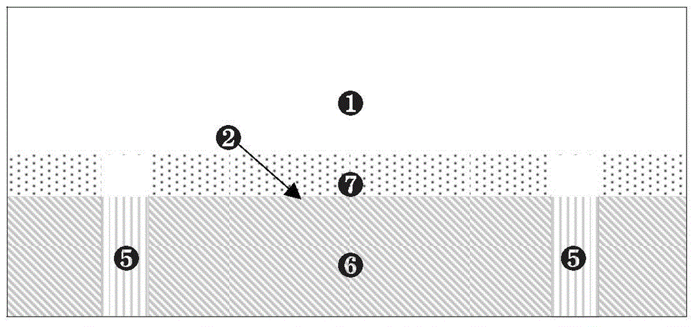
[0049] Example 1: Preparation of N-type composite emitter solar cells by laser treatment process image 3 The process route shown is carried out, and concrete steps are as follows:

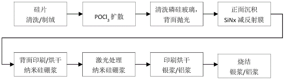
[0050] (1) Use a 125*125mm N-type CZ single crystal silicon wafer with a thickness of 160um and a silicon wafer substrate with a phosphorus doping concentration of 6x10 16 atm / cm 3 . Complete the following process according to the usual battery preparation process: 1. Silicon wafer cleaning and flocking; 2. POCl 3 Diffusion; 3. Clean the phosphosilicate glass and polish the back; 4. Deposit SiNx emission reduction film on the front;

[0051] (2) Print the nano-silicon boron paste on the back of the silicon wafer after (1) using the silver grid wire screen on the back of the conventional P-type battery and a conventional screen printing machine. The boron paste pattern is the same as the silver grid wire, and the printing thickness is 3.5 um. Nano silicon boron slurry is composed of 75 parts o...

Embodiment 2

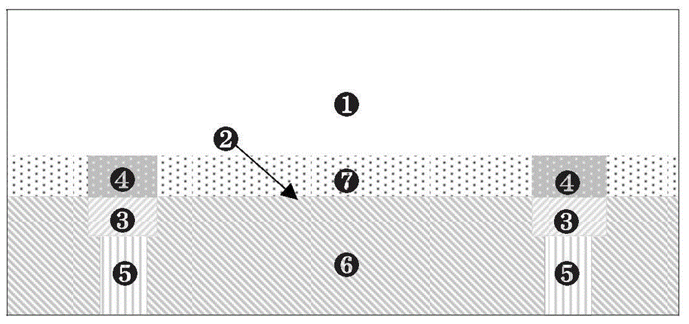
[0058] Embodiment 2: Utilize high-temperature treatment process to prepare N-type composite emitter solar cell, such as Figure 4 Shown:

[0059] (1) Use a 125*125mm N-type CZ single crystal silicon wafer with a thickness of 165um and a silicon wafer substrate with a phosphorus doping concentration of 6x10 16 atm / cc. According to the normal battery preparation process, complete the texturing of the front side of the silicon wafer and the polishing of the back side;

[0060] (2) Print the nano-silicon boron paste on the back of the silicon wafer after the process (1) using the silver grid wire screen on the back of the conventional P-type battery and a conventional screen printing machine. The boron paste pattern is the same as the silver grid wire, and the printing thickness is 2um . The nano-silicon boron slurry is composed of 80 parts of sandalwood and 20 parts of nano-silicon, the average particle diameter of the nano-silicon is 60nm, and the boron content is 8%.

[006...

Embodiment 3

[0067] Example 3: Preparation of improved P-type solar cells by laser treatment process image 3 The process route shown is carried out,

[0068] Specific steps are as follows:

[0069] (1) Use a 125*125mm P-type CZ monocrystalline silicon wafer with a thickness of 180um and a silicon wafer substrate with a boron doping concentration of 8x10 15 atm / cc. According to the normal battery preparation process, complete the production process of the front of the cell: 1. Silicon wafer cleaning and flocking; 2. POCl 3 Diffusion; 3. Clean and remove phosphorus silicon glass; 4. Deposit SiNx emission reduction film on the front side;

[0070] (2) Print the nano-silicon boron paste on the back of the silicon wafer after the process (1) using the silver grid screen and screen printing machine on the back of the conventional P-type battery. The pattern of the boron paste is the same as that of the silver grid, and the printing thickness is 2um. The nano-silicon boron slurry is composed...


PUM

PropertyMeasurementUnit
Particle sizeaaaaaaaaaa
Thicknessaaaaaaaaaa
Thicknessaaaaaaaaaa

Abstract

The invention discloses nano silicon boron slurry and a method for preparing N type composite emitter and an improved P type solar cell with the nano silicon boron slurry. The nano silicon boron slurry is used as a carrier, and local boron adulteration of the grating line coverage area of the solar cell back through laser or high-temperature treatment can be realized. The method is combined with the aluminum paste sintering process to prepare an N-type composite emitter cell when an N type cell is produced so that the problems that the ordinary aluminum paste sintering process only forms emitters in the aluminum paste coverage area and the emitters in the silver grating line coverage area are not continuous can be solved, and the photovoltaic conversion efficiency of the N type aluminum emitter cell is improved. The method is combined with the original aluminum paste sintering process to prepare the improved P type cell when the P type cell is produced so that the problems that the original P type cell only forms a back surface field in the aluminum slurry coverage area and the back surface field in the silver grating line coverage area is not continuous can be solved.

Description

technical field [0001] The invention belongs to the field of nanometer materials, and in particular relates to a nano-silicon-boron paste and its application in the preparation of solar cells, and the solar cells are N-type composite emitters or improved P-type solar cells. Background technique [0002] The emitter is the core part of the solar cell. Its role is to convert the light energy absorbed by the silicon wafer from sunlight into electrical energy. At present, common aluminum emitter cells form aluminum emitters by sintering aluminum paste. [0003] Aluminum emitter cell back structure such as figure 1 As shown, ① is the N-type silicon chip; ② is the back surface of the silicon chip; ⑤ is the silver grid line; ⑥ is the aluminum electrode; ⑦ is the aluminum emitter. [0004] Ordinary aluminum emitter cells only form emitters in the area covered by aluminum paste, and do not form emitters in the area covered by silver grid lines. The emitter is discontinuous in the...

Claims


Application Information

Patent Timeline
IPC IPC(8): H01L31/0224H01L31/18
CPCH01L31/022425Y02E10/50Y02P70/50
Inventor 蒋红彬沈晓东毛立中刘国钧
Owner 苏州金瑞晨科技有限公司
Why Eureka
Try Eureka