Light emitting diode using ITO regional sheet resistance change to improve current spreading and manufacturing method

A technology of light-emitting diodes and manufacturing methods, which is applied in the direction of circuits, electrical components, semiconductor devices, etc., can solve the problems of high cleanliness requirements for epitaxial layers, difficult epitaxial growth, and increased difficulty, so as to improve the uniformity of current expansion and improve the current Effect of expansion and reduction of production cost

Inactive Publication Date: 2015-05-13
SHANDONG INSPUR HUAGUANG OPTOELECTRONICS
View PDF11 Cites 7 Cited by
  • Summary
  • Abstract
  • Description
  • Claims
  • Application Information

AI Technical Summary

Problems solved by technology

The steps of this method are complicated, the epitaxial growth is difficult, and the cleanliness of the epitaxial layer after processing is high, which increases the difficulty of mass production.

Method used


Image

  • Light emitting diode using ITO regional sheet resistance change to improve current spreading and manufacturing method
  • Light emitting diode using ITO regional sheet resistance change to improve current spreading and manufacturing method
  • Light emitting diode using ITO regional sheet resistance change to improve current spreading and manufacturing method

Examples


Embodiment 1

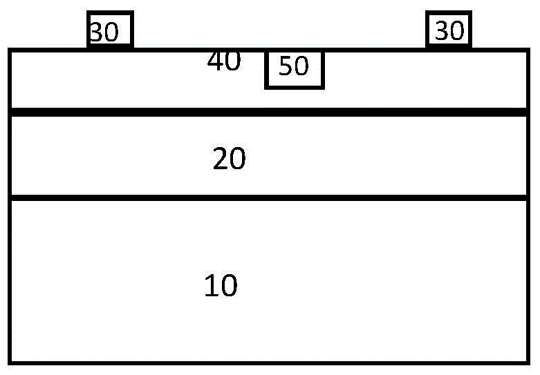
[0052] Embodiment 1. A method for improving the current spreading of light-emitting diodes by utilizing ITO regional square resistance changes, the described light-emitting diode structure includes an epitaxial wafer grown on a substrate 10, an ITO thin film 40 positioned on the epitaxial wafer, and a metal electrode 60 and passivation layer 70. Among them, the ITO film is made into three regions with different square resistance, low square resistance ITO region I, medium square resistance ITO region II and high square resistance ITO region III, and the square resistance of the low square resistance ITO region I is 5-10 ohms / square; the square resistance of ITO area II of the middle square resistance is 10-15 ohms / square; the square resistance of the high square resistance ITO area III is 50-70 ohms / square. The high square resistance ITO region III is located under the metal electrode, the area is smaller than the metal electrode pattern, and is 5-8 microns smaller than the ...

Embodiment 2

[0053] Embodiment 2. A light-emitting diode with improved current spreading and its manufacturing method

[0054] Step 1: Preparation of LED Epitaxial Wafer

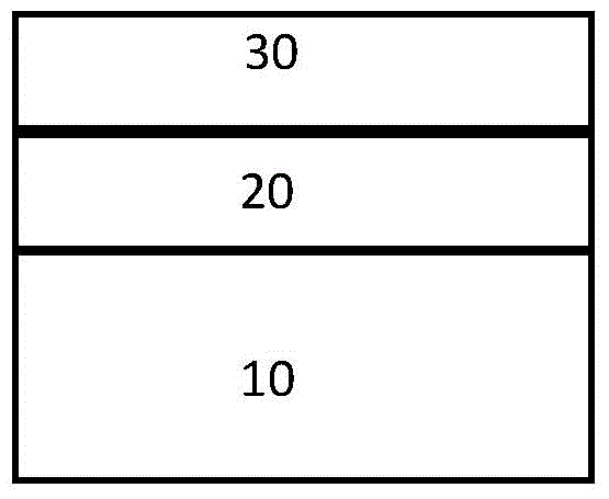
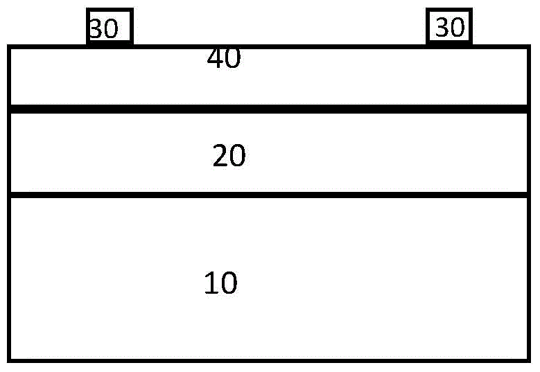
[0055] The epitaxial wafer includes GaN-based blue LED or AlGaInP quaternary red LED epitaxial wafer; the main structure of the epitaxial wafer includes a substrate 10 and an epitaxial layer 20 . Wherein the substrate is selected from sapphire, gallium arsenide, silicon or silicon carbide; the epitaxial layer includes a buffer layer, an N-type layer, a multiple quantum well, and a P-type layer;

[0056] Step 2: Growth of ITO film on the epitaxial wafer surface

[0057] Preparation of ITO thin films on the epitaxial layer, see figure 1 , the preparation method includes the use of secondary electron beam evaporation, plasma-assisted electron beam evaporation or magnetron sputtering, etc.; preferably, the electron beam evaporation ITO film 30, the evaporation rate is 1 to 1.5 angstroms / second, and the evaporation temperat...


PUM


Abstract

The invention relates to a light emitting diode using ITO regional sheet resistance change to improve current spreading and a manufacturing method. The light emitting diode comprises an epitaxial wafer grown on a substrate, an ITO film located on the epitaxial wafer, a metal electrode and a passivation layer; three ITO regions with different sheet resistances are located on the ITO film, a high-sheet resistance ITO region III is located below the metal electrode, a low-sheet resistance ITO region I is formed through a mask pattern, and the low-sheet resistance ITO region I extends to the edge through using the metal electrode as the center and has a branch shape. According to the light emitting diode using the ITO regional sheet resistance change to improve the current spreading and the manufacturing method, through improving or lowering the sheet resistance on the selective region of the ITO layer, the current spreading route guidance is realized, without increasing a current blocking layer, the current spreading uniformity of the light emitting diode can be improved through the regional treatment of the current spreading layer ITO, the light emitting efficiency is improved, and the high voltage of the chip is avoided.

Description

technical field [0001] The invention relates to a method for improving the current spread of a light-emitting diode by using the regional square resistance change of ITO, in particular to a light-emitting diode and a manufacturing method thereof, which belong to the technical field of light-emitting diode semiconductor materials. Background technique [0002] LED is the abbreviation of Light Emitting Diode in English. As a new type of lighting source, it has the advantages of small size, energy saving, cold light source, and fast response speed. The epitaxial structure of the blue LED chip is mainly gallium nitride GaN. Gallium nitride GaN is intrinsically N-type, and the epitaxial carrier concentration of unintentionally doped GaN is 10e14. N-type is generally doped with SiH4, and the carrier concentration is 10e19~ 10e20, the P-type doping of GaN is due to the passivation effect of H on Mg, resulting in low P-type doping concentration and high resistivity, and the longitud...

Claims


Application Information

Patent Timeline
Patent Type & Authority Applications(China)
IPC IPC(8): H01L33/14H01L33/00
CPCH01L33/14H01L33/00H01L33/005
Inventor 王德晓刘存志夏伟王成新任忠祥
Owner SHANDONG INSPUR HUAGUANG OPTOELECTRONICS
Why Eureka
Try Eureka