

Transparent organic light-emitting device and method for manufacturing same
A luminescence and electromechanical technology, applied in the direction of electrical solid devices, semiconductor/solid device manufacturing, electrical components, etc., can solve the problems of low light transmittance, easy cracks, thick transparent devices, etc., and achieve good compactness and uniformity , low deposition temperature and strong adhesion
- Summary
- Abstract
- Description
- Claims
- Application Information
AI Technical Summary
Problems solved by technology
Method used
Image

Examples
Embodiment 1
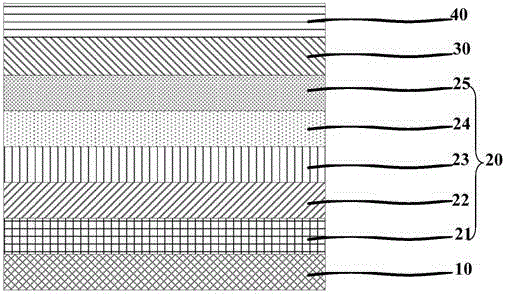
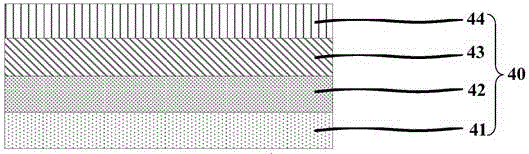
[0057] figure 1 It is the schematic diagram of the transparent organic electroluminescent device in embodiment 1; figure 1 As shown, the transparent organic electroluminescence device in Example 1 includes an ITO glass substrate (10), an organic light-emitting functional layer (20), a transparent cathode (30) and an encapsulation layer (40) stacked in sequence from bottom to top; The electroluminescent functional layer (20) includes a hole injection layer (21), a hole transport layer (22), a light emitting layer (23), an electron transport layer (24) and an electron injection layer (25) stacked in sequence from bottom to top . figure 2 yes figure 1 Schematic diagram of the structure of the encapsulation layer; such as figure 2As shown, the encapsulation layer (40) includes a mixed barrier layer (41), a first silicon oxynitride film layer (42), an inorganic barrier layer (43) and a second oxygen Silicon nitride film layer (44).
[0058] A method for preparing a transpare...
Embodiment 2
[0075] A method for preparing a transparent organic electroluminescent device, comprising the steps of:
[0076] (1), (2), (3) are the same as embodiment 1;
[0077] (4) Preparation of encapsulation layer:
[0078] a) Preparation of mixed barrier layer: The mixed barrier layer was prepared on the surface of the transparent cathode by vacuum evaporation method, and the vacuum degree was 5×10 -5 Pa, the evaporation rate is The mixed barrier layer materials include N,N'-diphenyl-N,N'-di(1-naphthyl)-1,1'-biphenyl-4,4'-diamine (NPB) and doped in Vanadium oxide (V 2 o 5 ) and aluminum (Al); vanadium oxide (V 2 o 5 ) is 40% by mole fraction, and aluminum (Al) is 30% by mole fraction; the thickness of the mixed barrier layer is 300nm;
[0079] b) Preparation of the first silicon oxynitride film layer: the first silicon oxynitride film layer was prepared on the surface of the mixed barrier layer by plasma enhanced chemical vapor deposition, the working pressure was 10Pa, the de...
Embodiment 3
[0084] A method for preparing a transparent organic electroluminescent device, comprising the steps of:
[0085] (1), (2), (3) are the same as embodiment 1;
[0086] (4) Preparation of encapsulation layer:
[0087] a) Preparation of mixed barrier layer: The mixed barrier layer was prepared on the surface of the transparent cathode by vacuum evaporation method, and the vacuum degree was 5×10 -5 Pa, the evaporation rate is Hybrid barrier materials include 8-hydroxyquinoline aluminum (Alq 3 ) and doped in 8-hydroxyquinoline aluminum (Alq 3 ) in tungsten oxide (WO 3 ) and nickel (Ni); tungsten oxide (WO 3 ) is 30% by mole fraction, nickel (Ni) is 10% by mole fraction; the thickness of the mixed barrier layer is 200nm;
[0088] b) Preparation of the first silicon oxynitride film layer: the first silicon oxynitride film layer was prepared on the surface of the mixed barrier layer by plasma enhanced chemical vapor deposition, the working pressure was 50Pa, the deposition tempe...
PUM
| Property | Measurement | Unit |
|---|---|---|
| Thickness | aaaaa | aaaaa |
| Thickness | aaaaa | aaaaa |
| Thickness | aaaaa | aaaaa |
Abstract
Description
Claims
Application Information