Organic electroluminescence device and manufacturing method for organic electroluminescence device

An electroluminescent device and electroluminescent technology, applied in the direction of electric solid device, semiconductor/solid state device manufacturing, electrical components, etc., can solve the problems of total reflection loss, refractive index difference, low light output performance, etc. Light Efficiency, Barrier Reduction Effect

Inactive Publication Date: 2015-05-27
OCEANS KING LIGHTING SCI&TECH CO LTD +2
View PDF0 Cites 0 Cited by
  • Summary
  • Abstract
  • Description
  • Claims
  • Application Information

AI Technical Summary

Problems solved by technology

[0003] In traditional light-emitting devices, only about 18% of the light inside the device can be emitted to the outside, while the rest will be consumed outside the device in other forms, and there is a difference in refractive index between the interfaces (such as between gla

Method used


Image

  • Organic electroluminescence device and manufacturing method for organic electroluminescence device
  • Organic electroluminescence device and manufacturing method for organic electroluminescence device

Examples


preparation example Construction

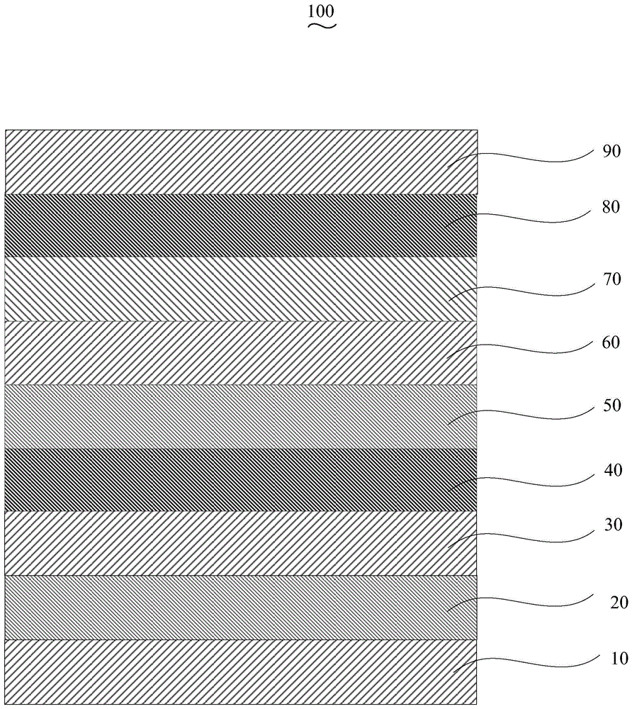
[0036] The preparation method of the organic electroluminescence device 100 of an embodiment, it comprises the following steps:

[0037] Step S110 , preparing the scattering layer 20 on the surface of the glass substrate 10 by electron beam evaporation.

[0038] The scattering layer 20 is formed on one side surface of the glass substrate 10 . The scattering layer 20 includes luminescent materials, zinc powder and rhenium compound materials, and the scattering layer 20 is prepared by electron beam evaporation on the surface of the glass substrate. The material of the luminescent material layer is selected from 4-(dinitrile methyl)-2 -Butyl-6-(1,1,7,7-tetramethyljulodine-9-vinyl)-4H-pyran (DCJTB), 9,10-di-β-naphthylene anthracene ( ADN), 4,4′-bis(9-ethyl-3-carbazolevinyl)-1,1′-biphenyl (BCzVBi), 8-hydroxyquinoline aluminum (Alq 3 ), the compound material of rhenium is selected from rhenium heptoxide (Re 2 o 7 ), rhenium dioxide (ReO 2 ) Rhenium trioxide (ReO 3 ) and rheniu...

Embodiment 1

[0058] The structure prepared in this example is glass substrate / Alq 3 :Zn:Re 2 o 7 / ITO / MoO 3 / NPB / Alq 3 / TAZ / CsF / Ag organic electroluminescent device, in this embodiment and the following embodiments, " / " indicates a layer, and ":" indicates doping.

[0059] The glass substrate is N-LASF44. After rinsing the glass substrate with distilled water and ethanol, soak it in isopropanol for one night. Prepare the scattering layer on the glass substrate. The scattering layer includes luminescent materials, zinc powder and rhenium compound materials. The scattering layer is prepared by electron beam evaporation on the surface of the glass substrate. The material is Alq 3 :Zn:Re 2 o 7 , Alq 3 , Zn and Re 2 o 7 The mass ratio is 25:1:5, and the thickness is 180nm. Then ITO is prepared on the scattering layer with a thickness of 100nm, which is prepared by magnetron sputtering; the hole injection layer is prepared by evaporation: the material is MoO 3 , with a thickness of 40...

Embodiment 2

[0066] The structure prepared in this example is glass substrate / ADN:Zn:ReO 2 / IZO / MoO 3 / TAPC / ADN / Bphen / CsN 3 / Al organic electroluminescent devices.

[0067] The glass substrate is N-LAF36. After rinsing the glass substrate with distilled water and ethanol, soak it in isopropanol for one night to prepare a scattering layer on the glass substrate. The scattering layer is prepared by electron beam evaporation on the surface of the substrate, and the material is ADN:Zn:ReO 2 , ADN, Zn and ReO 2 The mass ratio is 4:0.1:1, and the thickness is 400nm. Then IZO is prepared on the scattering layer with a thickness of 80nm, which is prepared by magnetron sputtering; the hole injection layer is evaporated, and the material is MoO 3 , with a thickness of 40nm; evaporated hole transport layer: the material is TAPC, with a thickness of 45nm; evaporated luminescent layer: the selected material is ADN, with a thickness of 8nm; evaporated electron transport layer, the material is Bphen...


PUM

PropertyMeasurementUnit
Thicknessaaaaaaaaaa
Particle sizeaaaaaaaaaa
Thicknessaaaaaaaaaa

Abstract

The invention discloses an organic electroluminescence device. The organic electroluminescence device comprises a glass substrate, a scattering layer, a positive pole, a hole-injection layer, a hole-transmission layer, a light-emitting layer, an electronic transmission layer, an electronic injection layer and a negative pole which are sequentially overlapped, wherein the scattering layer comprises a light-emitting material, zinc powder and a compound material of rhenium. The material of the light-emitting layer is selected from one and more of 4-(dicyanomethyl)-2-butyl-6-(1,1,7,7-tetramethyljulolidine-9-ethenyl)-4H-pyran, 9,10-di-beta-naphthyl anthracene, 4,4'-di(9-ethyl-3-vinylcarbazole)-1-1'-biphenyl and 8-hydroxyquinoline aluminum. The compound material of rhenium is selected from one and more of rhenium oxide, rhenium oxide, rhenium trioxide and rhenium chloride. The organic electroluminescence device is relatively high in light-emitting efficiency. The invention also provides a manufacturing method for the organic electroluminescence device.

Description

technical field [0001] The invention relates to an organic electroluminescence device and a preparation method thereof. Background technique [0002] The luminescence principle of organic electroluminescent devices is based on the action of an external electric field, electrons are injected from the cathode to the lowest unoccupied molecular orbital (LUMO) of organic matter, and holes are injected from the anode to the highest occupied molecular orbital (HOMO) of organic matter. Electrons and holes meet, recombine, and form excitons in the light-emitting layer. Excitons migrate under the action of an electric field, transfer energy to the light-emitting material, and excite electrons to transition from the ground state to the excited state. The excited state energy is deactivated by radiation to generate photons , releasing light energy. [0003] In traditional light-emitting devices, only about 18% of the light inside the device can be emitted to the outside, while the res...

Claims


Application Information

Patent Timeline
IPC IPC(8): H01L51/50H01L51/52H01L51/54H01L51/56
Inventor 周明杰黄辉张振华王平
Owner OCEANS KING LIGHTING SCI&TECH CO LTD
Why Eureka
Try Eureka