Large-area cadmium sulfide film preparing method

A thin-film preparation and cadmium sulfide technology, which is applied in the fields of final product manufacturing, sustainable manufacturing/processing, semiconductor/solid-state device manufacturing, etc., can solve the problems of environmental pollution of ammonia water, waste of resources, etc., achieve low reaction temperature, avoid corrosion, and improve performance good effect

Inactive Publication Date: 2015-06-10
TIANJIN UNIVERSITY OF TECHNOLOGY
View PDF0 Cites 1 Cited by
  • Summary
  • Abstract
  • Description
  • Claims
  • Application Information

AI Technical Summary

Problems solved by technology

However, excessive use of ammonia water is likely to cause environmental pollution and waste of resources.

Method used


Image

  • Large-area cadmium sulfide film preparing method
  • Large-area cadmium sulfide film preparing method
  • Large-area cadmium sulfide film preparing method

Examples


Embodiment 1

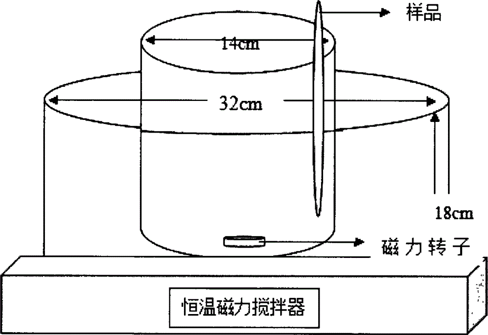
[0047] A large-area cadmium sulfide thin film is prepared by using a chemical water bath method based on a copper indium gallium selenide substrate. The preparation steps are as follows:

[0048] Preparation of CIGS substrate: Firstly, the CIGS absorbing layer prepared on the glass substrate must be obtained.

[0049] 1) Cleaning of soda lemon glass

[0050] ① Soak a 10cm×10cm soda glass in heavy potassium hydroxide solution (a solution made of 300 grams of potassium hydroxide and 3 liters of deionized water) for 2 hours; ② Put the rinsed soda glass in a concentration of 99.5 % acetone solution, put it into an ultrasonic cleaning machine for cleaning with an ultrasonic frequency of 50kHz and a time of 30min, which can be properly heated to 40°C; ③ Take the soda glass out of the acetone solution and rinse it with deionized water; ④ Clean the washed Soda-lemon glass substrates were cleaned with alcohol and dried with nitrogen.

[0051] 2) Preparation of molybdenum back contact...

Embodiment 2

[0064] A large-area cadmium sulfide thin film is prepared by using a chemical water bath method based on a copper indium gallium selenide substrate. The preparation steps are as follows:

[0065] Preparation of CIGS substrate: Firstly, the CIGS absorbing layer prepared on the glass substrate must be obtained.

[0066] 1) Cleaning of soda lemon glass

[0067] ① Soak a 10cm×10cm soda glass in heavy potassium hydroxide solution (a solution made of 300 grams of potassium hydroxide and 3 liters of deionized water) for 2 hours; ② Put the rinsed soda glass in a concentration of 99.5 % acetone solution, put it into an ultrasonic cleaning machine for cleaning with an ultrasonic frequency of 50kHz and a time of 30min, which can be properly heated to 40°C; ③ Take the soda glass out of the acetone solution and rinse it with deionized water; ④ Clean the washed Soda-lemon glass substrates were cleaned with alcohol and dried with nitrogen.

[0068] 2) Preparation of molybdenum back contact...


PUM

PropertyMeasurementUnit
heightaaaaaaaaaa
diameteraaaaaaaaaa
thicknessaaaaaaaaaa

Abstract

Disclosed is a large-area cadmium sulfide film preparing method adopting a chemical immersion method on the basis of a copper-indium-gallium-selenium substrate. The large-area cadmium sulfide film preparing method is characterized by including the steps of preparing a molybdenum electrode on a glass substrate by a magnetron sputtering method, preparing a copper-indium-gallium-selenium film by a co-evaporation method, preparing a large-area CdS (cadmium sulfide) film on the surface of a composite substrate by the chemical immersion method under a low-ammonia condition, and regulating and controlling evenness in film growth by a rotor. The large-area cadmium sulfide film preparing method adopting the chemical immersion method on the basis of the copper-indium-gallium-selenium substrate has the advantages of good crystallization quality, high density and no pin hole in crystallization, good crystal adhesiveness, high crystal transmittance, simplicity, easiness in implementation, benefit to large-scale popularization and application and vitally important application prospect in industrial production.

Description

technical field [0001] The invention relates to the technical field of thin-film solar cells, especially in the field of thin-film solar cells with copper indium gallium selenide as the absorbing layer. The cadmium sulfide thin film is used as a key layer as a buffer layer to adjust the band gap gradient and as an n-type semiconductor material. Background technique [0002] Cadmium sulfide (CdS) is a semiconductor material with great research potential and a wide range of applications. It is easy to prepare, cost-effective and suitable for large-scale production. In addition, cadmium sulfide also has a variety of utilization forms. It can be made into zero-dimensional materials such as atomic clusters and nanoparticles, and can be used to prepare a variety of quantum devices; it can be prepared into one-dimensional nanomaterials such as nanowires, nanorods, nanoflowers, nanobelts, and nanohollow spheres. , can be applied to nanowire lasers, logic gate computing circuits, na...

Claims


Application Information

Patent Timeline
Patent Type & Authority Applications(China)
IPC IPC(8): H01L31/18
CPCH01L21/02422H01L21/02485H01L21/02499H01L21/02557H01L31/03925Y02P70/50
Inventor 薛玉明尹富红潘洪刚刘君郭晓倩宋殿友朱亚东李鹏海冯少君张嘉伟刘浩高林航伟乔在祥李鹏宇王玉昆曲慧楠
Owner TIANJIN UNIVERSITY OF TECHNOLOGY
Why Eureka
Try Eureka