Organic light-emitting device and manufacturing method thereof
An electroluminescent device and electroluminescent technology, which are applied in the fields of electro-solid devices, semiconductor/solid-state device manufacturing, electrical components, etc., can solve the problems of reduced luminous efficiency, low probability of exciton recombination, and difficulty of luminous efficiency to meet the needs of use.
- Summary
- Abstract
- Description
- Claims
- Application Information
AI Technical Summary
Problems solved by technology
Method used
Image

Examples
preparation example Construction
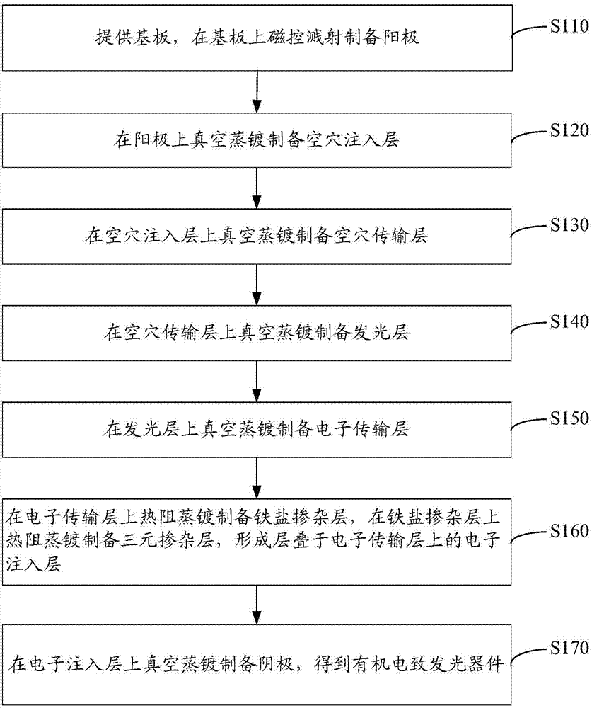
[0061] see figure 2 , a method for preparing an organic electroluminescent device according to an embodiment, comprising the following steps S110 to S170.
[0062] Step S110: providing a substrate, and preparing an anode on the substrate by magnetron sputtering.
[0063] The substrate is a transparent substrate, preferably glass.
[0064] After the substrate was rinsed with distilled water and ethanol in sequence, it was soaked overnight in isopropanol. Then take it out and dry it for later use.
[0065] The anode is prepared on a dry and clean substrate by magnetron sputtering process. The acceleration voltage of magnetron sputtering is 300V-800V, the magnetic field strength is 50G-200G, and the power density is 1W / cm 2 ~40W / cm 2 .
[0066] The anode is indium tin oxide film (ITO), aluminum-doped zinc oxide film (AZO) or indium-doped zinc oxide film (IZO), preferably indium tin oxide film (ITO).
[0067] The thickness of the anode is 50 nm to 300 nm, preferably 120 nm...
Embodiment 1
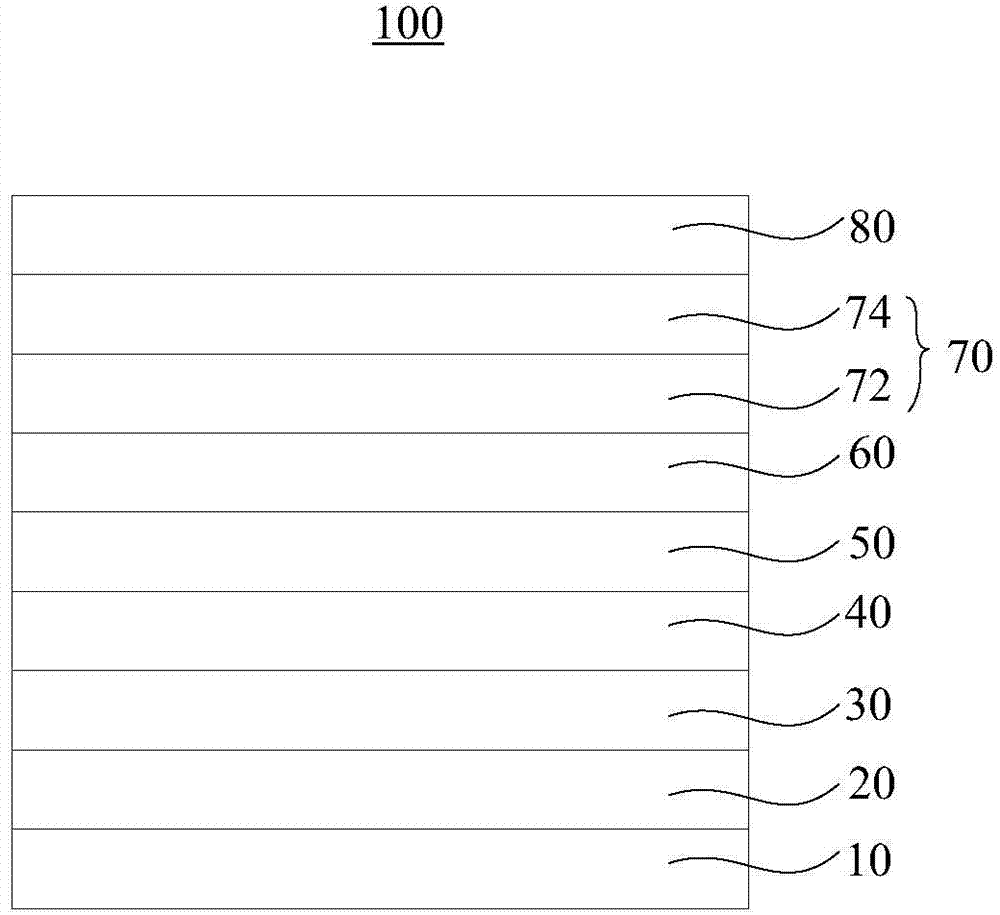
[0105] The preparation structure is Glass / ITO / MoO 3 / NPB / BCzVBi / TPBi / FeCl 3 :PC61BM / MgPc:BCzVBi:C60 / Ag Organic Electroluminescent Device
[0106] 1. Provide glass as the substrate, denoted as Glass. Rinse the glass with distilled water and ethanol, soak it in isopropanol overnight, then take it out and dry it for later use;
[0107] 2. The anode is prepared on a dry and clean substrate by magnetron sputtering. The acceleration voltage of magnetron sputtering is 700V, the magnetic field strength is 120G, and the power density is 25W / cm 2 , the material of the anode is indium tin oxide (ITO), the anode is expressed as ITO, and the thickness of the anode is 120 nanometers;
[0108] 3. Prepare a hole injection layer on the anode by vacuum evaporation. The working pressure is 8×10 -4 Pa, the evaporation rate is 0.2nm / s. The material of the hole injection layer is molybdenum trioxide (MoO 3 ), the hole injection layer is denoted as MoO 3 , the thickness of the hole injectio...
Embodiment 2
[0117] The preparation structure is Glass / IZO / WO 3 / NPB / Alq 3 / TAZ / FeBr 3 :C70 / MgPc:Alq 3 :C70 / Al Organic Electroluminescent Devices
[0118] 1. Provide glass as the substrate, denoted as Glass. Rinse the glass with distilled water and ethanol, soak it in isopropanol overnight, then take it out and dry it for later use;
[0119] 2. The anode is prepared on a dry and clean substrate by magnetron sputtering. The acceleration voltage of magnetron sputtering is 300V, the magnetic field strength is 50G, and the power density is 40W / cm 2 , the material of the anode is indium-doped zinc oxide film (IZO), the anode is expressed as IZO, and the thickness of the anode is 300 nanometers;
[0120] 3. Prepare a hole injection layer on the anode by vacuum evaporation. The working pressure is 2×10 -3 Pa, the evaporation rate is 1nm / s. The material of the hole injection layer is tungsten trioxide (WO 3 ), the hole injection layer is denoted as WO 3 , the thickness of the hole injec...
PUM
 Abstract
Description
Claims
Application Information
 - R&D
- Intellectual Property
- Life Sciences
- Materials
- Tech Scout
- Unparalleled Data Quality
- Higher Quality Content
- 60% Fewer Hallucinations
Browse by: Latest US Patents, China's latest patents, Technical Efficacy Thesaurus, Application Domain, Technology Topic, Popular Technical Reports.
© 2025 PatSnap. All rights reserved.Legal|Privacy policy|Modern Slavery Act Transparency Statement|Sitemap|About US| Contact US: help@patsnap.com