Graphene nanoribbon array terahertz sensor based on optical waveguide

A graphene nanoribbon and optical waveguide technology, applied in the field of terahertz sensors, can solve the problems of small effective photosensitive surface and low signal light energy utilization rate, achieve high carrier mobility, improve light energy utilization rate, and sensitivity high effect

Inactive Publication Date: 2015-07-22
CHONGQING UNIV
View PDF9 Cites 17 Cited by
  • Summary
  • Abstract
  • Description
  • Claims
  • Application Information

AI Technical Summary

Problems solved by technology

However, there are still many problems in the production of large-area and stable graphene materials in the existing technology, resulting in a small effective photosensitive surface of graphene THz detectors, and a small utilization rate of light energy for signals, which limits its development to practical applications.

Method used


Image

  • Graphene nanoribbon array terahertz sensor based on optical waveguide
  • Graphene nanoribbon array terahertz sensor based on optical waveguide
  • Graphene nanoribbon array terahertz sensor based on optical waveguide

Examples


Embodiment Construction

[0023] Below in conjunction with accompanying drawing and embodiment the present invention will be further described:

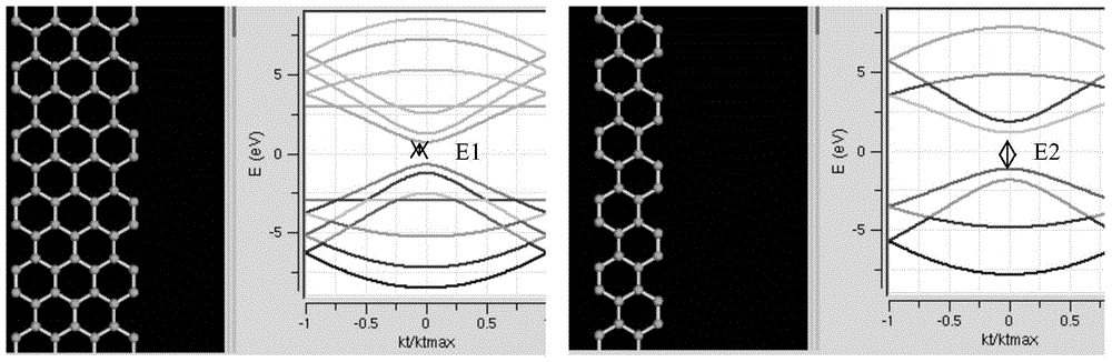
[0024] figure 1 Schematic diagram for single-layer graphene nanostructure and tuned bandgap. The biggest problem in the application of graphene materials as semiconductor optoelectronic materials is the zero energy gap characteristic of graphene, so the regulation of graphene energy gap has become the primary problem in the application of graphene optoelectronic devices. Lateral confinement, vertical electromagnetic field, molecular doping, strain and other methods have been applied to the regulation of graphene energy gap. Among them, the method of using graphene nanoribbons to generate an energy gap has become the best means to regulate the energy gap of graphene because it has little influence on the properties of graphene materials. figure 1 The left and right sides show the graphene nanoribbon structure and energy gap correspondence of different widths...


PUM


Abstract

The invention relates to a terahertz sensor, in particular to a graphene nanoribbon array terahertz sensor based on optical waveguide. The graphene nanoribbon array terahertz sensor comprises a bottom grid, a low-resistivity silicon substrate, a lower insulation layer, a graphene nanoribbon array, a source leak electrode, an upper insulation layer, a top grid, an optical waveguide structure, an incidence coupling raster, an emitting coupling raster and a driving circuit, wherein the lower insulation layer, the graphene nanoribbon array, the source leak electrode, the upper insulation layer, the top grid, the optical waveguide structure, the incidence coupling raster, the emitting coupling raster and the driving circuit are arranged on the substrate; the graphene materials have the photoelectric characteristics of high carrier mobility, electronic scattering-free transmission and adjustable energy gap and adopt the graphene nanoribbon and p-i-n photoelectric detecting structure. By means of characteristics of collection, transmission and gathering of the optical waveguide, and the composite structure of the large-area optical waveguide and the graphene nanoribbon array is designed. The terahertz sensor has the advantages of high light energy utilization rate, high sensitivity, fast response, simple operation and structure at the room temperature, convenience in integration and small size, can be widely applied to the fields of security check, drug smuggling investigation, counter terrorism, medical imaging, nondestructive testing, electronic countermeasures, radar, remote sensing, outer space wideband communication and the like.

Description

technical field [0001] The present invention relates to a terahertz sensor, more specifically, the present invention relates to a graphene terahertz sensor based on an optical waveguide. technical background [0002] Compared with microwaves and light waves, terahertz waves have the characteristics of low photon energy, high temporal and spatial coherence, and strong penetration. In recent years, the demand for portable terahertz imaging / spectroscopy systems has become increasingly urgent in the fields of anti-terrorism and anti-terrorism, security inspection, anti-drug and on-site non-destructive testing. The miniaturization of terahertz systems and equipment puts forward requirements such as miniaturization and room temperature operation for its core components, THz source and THz detector. [0003] At present, the commonly used THz detection technology can be divided into coherent detection technology and direct detection technology. Compared with the expensive and comp...

Claims


Application Information

Patent Timeline
Patent Type & Authority Applications(China)
IPC IPC(8): H01L27/144H01L31/115H01L31/028
Inventor 温中泉张智海陈李陈刚
Owner CHONGQING UNIV
Why Eureka
Try Eureka