
Nanocrystal particle, process for synthesizing the same, and device comprising the same

A technology of nanocrystal particles and nanocrystals, applied in nanotechnology, nanooptics, nanotechnology, etc.

Active Publication Date: 2015-08-05
SAMSUNG ELECTRONICS CO LTD
View PDF7 Cites 26 Cited by
  • Summary
  • Abstract
  • Description
  • Claims
  • Application Information

AI Technical Summary

Problems solved by technology

[0006] Nanocrystalline particles can exhibit enhanced luminous efficiency, but there remains a need to provide improved quantum yields to provide improved luminous efficiency

Method used


Image

  • Nanocrystal particle, process for synthesizing the same, and device comprising the same
  • Nanocrystal particle, process for synthesizing the same, and device comprising the same
  • Nanocrystal particle, process for synthesizing the same, and device comprising the same

Examples


example 1

[0139] Reference Example 1: Preparation of InP Core

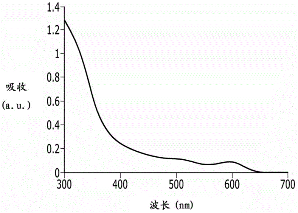
[0140] Put 0.2 millimoles (mmol) (0.058 grams (g)) of indium acetate, 0.6 mmol (0.15 g) of palmitic acid, and 10 milliliters (mL) of 1-octadecene in a flask, and in a vacuum state at 120 ° C After heating for one hour, the atmosphere in the flask was replaced with N 2 After replacement, heat to 280°C. Then, a mixed solution of 0.1 mmol (29 microliters (μL)) of tris(trimethylsilyl)phosphine (“TMS3P”) and 0.5 mL of trioctylphosphine (“TOP”) was quickly injected thereinto, and the reaction proceeded 20 minutes. The reaction mixture was then rapidly cooled to room temperature, and acetone was added to it to precipitate the nanocrystals, which were then separated by centrifugation and redispersed in toluene. The first UV absorption maximum wavelength of the thus prepared InP core nanocrystal is 560nm-590nm.

example 2

[0141] Reference Example 2: Preparation of InP core including boron and fluorine

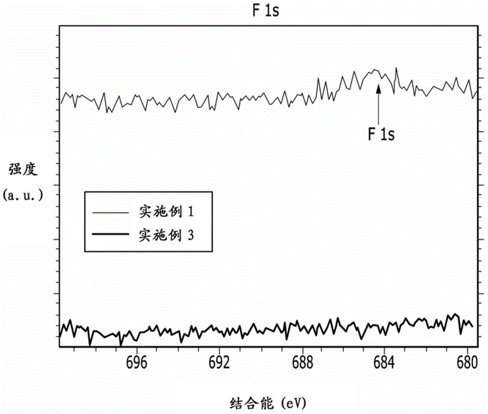
[0142] 0.2 mmol (0.058 g) of indium acetate, 0.6 mmol (0.15 g) of palmitic acid and 10 mL of 1-octadecene were placed in a flask, and heated at 120° C. for one hour under vacuum, and then the atmosphere in the flask was replaced with N 2 replacement. The reaction solution was heated to 280 °C, and 0.7 mmol of ethoxyethane-trifluoroborane (BF 3 .Et 2O). Subsequently, a mixed solution of 0.1 mmol of tris(trimethylsilyl)phosphine (“TMS3P”) and 0.5 mL of trioctylphosphine (“TOP”) was rapidly injected thereto. The reaction was carried out for 20 minutes. The reaction mixture was then rapidly cooled to room temperature, and acetone was added to it to precipitate the nanocrystals, which were then separated by centrifugation and dispersed in toluene. The InP semiconductor nanocrystal thus prepared had a light emission peak similar to that of the nanocrystal of Reference Example 1. The results of ...

Embodiment 1

[0143] Embodiment 1: Preparation of InP / BF_ZnS nano crystal particles

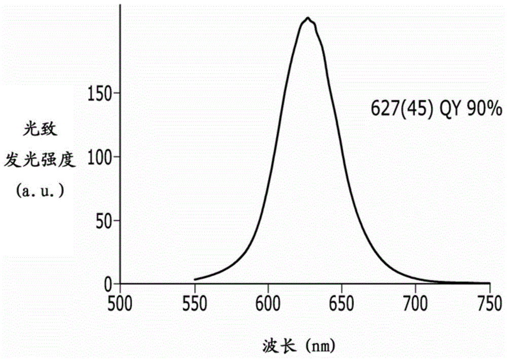
[0144] 1.2mmol (0.224g) of zinc acetate, 2.4mmol (0.757g) of oleic acid and 10mL of trioctylamine were placed in a flask, and heated at 120°C for one hour under vacuum, and then the atmosphere in the flask was replaced with N 2 replacement. Then, the reaction solution was heated to 280°C, and borane dimethylamine (BH 3 NMe 2 H) 0.07 mL of a 0.2 M toluene solution, and then 1 mL of the InP core solution prepared in Reference Example 1 was added thereto (OD = optical density of first exciton absorption, OD: 0.3, measured when diluted 100 times with toluene) And then add 2.4mmol S-TOP. After injecting it quickly with a mixture of 0.14 mmol HF (6 μL of aqueous solution) and 1.5 mL of trioctylamine ("TOA"), the reaction was carried out for 2 hours. The reaction mixture was then rapidly cooled to room temperature, and ethanol was added thereto to precipitate the nanocrystals, which were then separated by cen...


PUM


Abstract

A nanocrystal particle including: a semiconductor material; boron and optionally fluorine, wherein the particle has an organic ligand bound to a surface thereof, the boron is present as being doped in the particle or as a metal boride and the fluorine is present as being doped in the particle or as a metal fluoride.

Description

[0001] Cross References to Related Applications [0002] This application claims the priority and benefit of Korean Patent Application No. 10-2014-0013240 filed on February 5, 2014 and Korean Patent Application No. 10-2015-0016823 filed on February 3, 2015, both of which The contents are hereby incorporated by reference in their entirety. technical field [0003] Nanocrystalline particles, methods of synthesis thereof, and devices incorporating the same are disclosed. Background technique [0004] Unlike bulk materials, nanocrystals have unique physical properties (eg, bandgap and melting point) as a function of their particle size. For example, semiconductor nanocrystals (also known as quantum dots) are semiconductor materials that have a crystalline structure and dimensions of a few nanometers. Semiconductor nanocrystals have very small sizes and large surface areas per unit volume, and can exhibit quantum confinement effects. Therefore, semiconductor nanocrystals have ...

Claims


Application Information

Patent Timeline
Patent Type & Authority Applications(China)
IPC IPC(8): C09K11/72C09K11/70B82Y20/00B82Y30/00B82Y40/00
CPCC09K11/025Y10S977/95B82Y40/00Y10S977/773Y10S977/892B82Y20/00Y02E10/52C09K11/70
Inventor 田信爱章效淑元裕镐张银珠
Owner SAMSUNG ELECTRONICS CO LTD
Learn More