High-voltage semiconductor device and manufacturing method thereof

A manufacturing method and semiconductor technology, applied in semiconductor/solid-state device manufacturing, semiconductor devices, electrical components, etc., can solve the problems of large electric field on the surface of the device, high requirements for process control, and high requirements for process equipment

Active Publication Date: 2017-07-28
HANGZHOU SILAN MICROELECTRONICS
View PDF7 Cites 0 Cited by
  • Summary
  • Abstract
  • Description
  • Claims
  • Application Information

AI Technical Summary

Problems solved by technology

However, this traditional structure has the following disadvantages: After implantation to form a deep high-voltage well 4, in order to form a junction depth of more than 10 μm, it usually requires a high-temperature pushing junction of more than 1200 degrees and lasting more than 30-40 hours, which is harmful to the process equipment. High requirements and low process efficiency
[0005] refer to Figure 1B , in the prior art, the source fingertip part on the high-voltage device layout generally adopts a horseshoe-shaped buffer layer structure, but this structure wastes the device area on the one hand, and on the other hand cannot conduct electricity, so that the device channel cannot be fully utilized
This simple double-resurf structure, that is, only the structure of the high-voltage well 4 and the field drop layer 7, has a small process window, high requirements for process control, and a large electric field on the surface of the device, which will affect the reliability of the device. sex

Method used


Image

  • High-voltage semiconductor device and manufacturing method thereof
  • High-voltage semiconductor device and manufacturing method thereof
  • High-voltage semiconductor device and manufacturing method thereof

Examples


no. 1 example

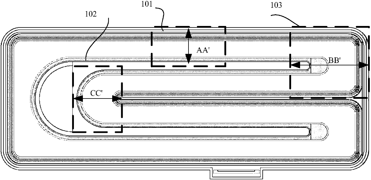
[0124] refer to figure 2 , figure 2 The complete layout of the semiconductor device according to the first embodiment is shown, and the device layout of this embodiment is an interdigitated layout to obtain sufficient current capability. The layout mainly includes a straight edge portion 101 , a source fingertip portion 102 , a drain fingertip portion 103 and other portions. In different regions of the layout, the cross-sectional structure of the device is not exactly the same. Among them, the straight edge part 101 is arranged along a straight line and is the main conductive part of the device; the drain finger tip part 103 and the source finger tip part 102 can be collectively referred to as the chamfered part. Along a single straight line, it has an arc or corner area. The main function of the chamfered part is to provide the transition of the complete device layout and ensure the effective withstand voltage of the device.

[0125] refer to image 3 , image 3 for ...

no. 2 example

[0139] In the second embodiment, the formation process of the buried layer will be described in detail.

[0140] refer to Figure 5A and Figure 5B , which shows the formation process of the buried layer 2 of a nonlinear variable doping structure. Such as Figure 5A As shown, ion implantation is performed using a mask 20 as a mask, wherein the mask 20 may be patterned photoresist or other suitable mask materials. After the ion implantation, the edge portion of the buried layer 2 can be expanded laterally by high-temperature pushing junction, so as to obtain the buried layer 2 with a nonlinear graded doping structure. Figure 5B Shown is a topography diagram of the buried layer 2 after ion implantation and annealing, wherein the buried layer 2 is a single doped region.

[0141] refer to Figure 6A and Figure 6B , which shows a formation process of the buried layer 2 adopting a linear variable doping structure. Figure 6A As shown, ion implantation is performed using a m...

no. 3 example

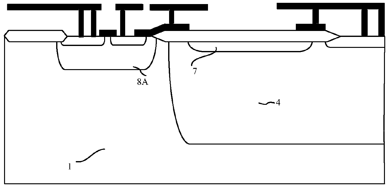
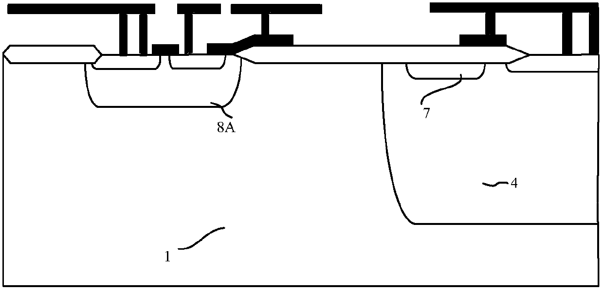
[0144] refer to Figure 8 , Figure 8 A schematic cross-sectional structure diagram of a straight-side portion of the high-voltage semiconductor device of the third embodiment is shown. figure 2 The straight edge part 101 in can be obtained by cutting along AA' Figure 8 The sectional view shown. Figure 8 The structure shown and image 3 The structures shown are basically the same, except that the P-type doped buried layer 2 adopts a linearly variable doping structure, including a plurality of mutually separated doping regions. The advantage of this is: without increasing the complexity of the process, only slight changes are made on the layout, so that the buried layer 2 forms a linear variable doping structure, thereby optimizing the electric field distribution at the source end, improving the reliability of the device, and The linearly variable doping processes of the source fingertip parts are matched to each other.


PUM


Abstract

The invention provides a high voltage semiconductor device and a manufacture method thereof; the device comprises a first dope type semiconductor substrate, a second dope type epitaxial layer arranged on the semiconductor substrate, a second dope type high voltage well positioned in the epitaxial layer, a second dope type deep well positioned in the high voltage well, a first dope type reduced-field layer positioned on the surface of the epitaxial layer and / or in the epitaxial layer (wherein at least a part of the reduced-field layer is positioned in the deep well), a first dope type first well parallel to the high voltage well and positioned in the epitaxial layer, a second dope type source electrode ohmic contact zone arranged in the first well, a drain electrode ohmic contact zone arranged in the deep well, a grid electrode close to the source electrode ohmic contact zone and at least covering the epitaxial layer between the source electrode ohmic contact zone and the high voltage well. The high voltage semiconductor device and the manufacture method thereof can effectively reduce technical manufacture difficulty, improve device parameter characteristics, and improve device reliability.

Description

technical field [0001] The invention relates to a semiconductor device and a manufacturing process, in particular to a high-voltage semiconductor device and a manufacturing method thereof. Background technique [0002] High-voltage BCD (Bipolar-CMOS-DMOS) technology generally refers to BCD technology with a withstand voltage of more than 100V, and is currently widely used in AC-DC power supplies, LED drivers and other fields. Generally, power devices are required to withstand a voltage ranging from 500V to 800V. [0003] The LDMOS (lateral double diffusion MOS) transistor device is a lateral high-voltage device, which is generally used as a driving device for the following modules in AC applications. Usually, all electrodes of LDMOS transistor devices are on the surface of the device, which is convenient for integrated design with low-voltage circuit parts. In current applications, such as LED and AC-DC products, the area of ​​LDMOS transistors may account for more than ha...

Claims


Application Information

Patent Timeline
Patent Type & Authority Patents(China)
IPC IPC(8): H01L29/06H01L29/78H01L21/336
CPCH01L29/06H01L29/7816
Inventor 姚国亮张邵华吴建兴
Owner HANGZHOU SILAN MICROELECTRONICS
Why Eureka
Try Eureka