
Method for growing epitaxial wafer of GaN-based light emitting diode

A light-emitting diode and growth method technology, which is applied in the growth field of GaN-based light-emitting diode epitaxial wafers, can solve the problems of weak current expansion ability of NP layer, poor antistatic ability of epitaxial wafers, and reduction of light output from the front of the chip, so as to ensure the front The effect of light output, uniform crystal laying, and better current expansion ability

Active Publication Date: 2015-10-07
HC SEMITEK SUZHOU
View PDF3 Cites 4 Cited by
  • Summary
  • Abstract
  • Description
  • Claims
  • Application Information

AI Technical Summary

Problems solved by technology

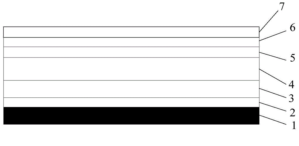
[0003] The existing GaN-based LED epitaxial wafer mainly includes a buffer layer, an N-type layer, a multi-quantum well layer, a P-type layer and a P-type contact layer grown on the substrate in sequence, wherein the multi-quantum well layer includes InGaN quantum wells layer and GaN quantum barrier layer, usually, the growth pressure of the P-type layer will not be higher than 200torr, the crystal quality of the P-type layer grown by this low-pressure growth method is poor, and the lattice mismatch between the substrate and the epitaxial wafer is caused The defect density, and the defect density caused by the lattice mismatch between the InGaN quantum well layer and the GaN quantum barrier layer in the MQW layer, will be further amplified in the P-type layer, thereby increasing the NP(N-type layer The leakage channel between the NP layer and the P-type layer), the current spreading ability of the NP layer becomes weaker, the breakdown point increases, and the antistatic ability of the epitaxial wafer is relatively poor. In order to ensure the antistatic ability of the LED device, the P-type layer is usually However, due to the light-absorbing characteristics of the P-type layer, the P-type layer with a thickness of not less than 80nm will absorb more light, which will reduce the amount of light emitted from the front of the chip and reduce the device’s performance. Luminous efficiency

Method used


Image

  • Method for growing epitaxial wafer of GaN-based light emitting diode
  • Method for growing epitaxial wafer of GaN-based light emitting diode

Examples


Embodiment 1

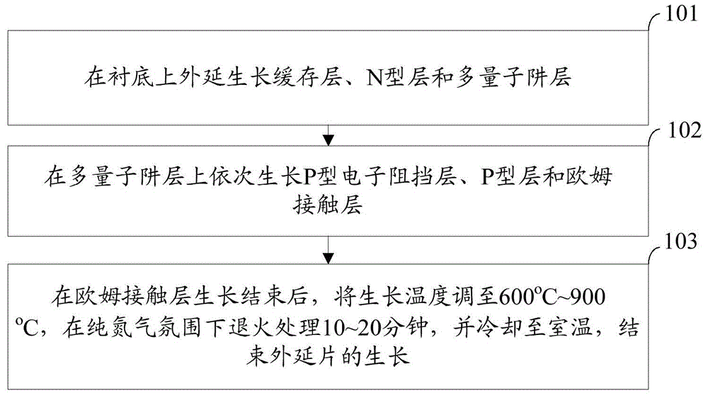
[0024] An embodiment of the present invention provides a method for growing a GaN-based light-emitting diode epitaxial wafer, see figure 1 , the method includes:

[0025] Step 101: epitaxially growing a buffer layer, an N-type layer and a multi-quantum well layer on the substrate.

[0026] Wherein, the substrate is a material suitable for the growth of gallium nitride and other semiconductor epitaxial materials, such as gallium nitride single crystal, sapphire, single crystal silicon, silicon carbide single crystal, and the like.

[0027] Specifically, the buffer layer may be one or more layers (ie composite buffer layer). When the buffer layer is a composite buffer layer, it may include a low temperature buffer layer and a high temperature buffer layer. As an example, the composition of the low-temperature buffer layer can be GaN, with a thickness of 15nm to 30nm, preferably 20nm; the composition of the high-temperature buffer layer can be high-temperature undoped GaN, with...

Embodiment 2

[0041] An embodiment of the present invention provides a method for growing a GaN-based light-emitting diode epitaxial wafer. In this embodiment, the N-type layer includes a high-temperature N-type GaN layer and a high-temperature N-type GaN current spreading layer. The growth temperature of the high-temperature N-type GaN layer is It is 1100℃, and the doping concentration of Si is 5×10 18 cm -3 , the growth temperature of the high-temperature N-type GaN current spreading layer is 1100°C, and the doping concentration of Si is 2×10 17 cm -3 , the multi-quantum well layer is composed of twelve 3nm In 0.18 Ga 0.82 A multilayer quantum well composed of N quantum well layer and 12 10.5nm GaN quantum barrier layers, and the P-type electron blocking layer is P-type Al 0.16 Ga 0.84 N layer, in which the doping concentration of Mg is 5×10 17 cm -3 , the P-type layer is a Mg-doped GaN layer, and the concentration of Mg doping is 5×10 19 cm -3 , the growth pressure is 600torr, t...

Embodiment 3

[0045] The embodiment of the present invention provides a method for growing a GaN-based light-emitting diode epitaxial wafer, wherein the buffer layer, N-type layer, multiple quantum well layer, P-type electron blocking layer and ohmic contact layer are the same as in Embodiment 2, and the same as in Embodiment 2. The difference between the two is that the growth pressure of the P-type layer is changed to 700torr, and the flow rate of TMGa is adjusted to 20sccm.

[0046] Similarly, after the growth of the epitaxial wafer is completed, semiconductor processing techniques such as cleaning, deposition, and photolithography are continued to be performed on the epitaxial wafer to produce an LED chip with a single chip size of 10×25 mil, and the LED chip is subjected to the same conditions as in Example 2. The results obtained are: the test current is 60mA, the operating voltage is 3.05V, the brightness is 110mw, and the 4KV antistatic ability is 93%. Compared with the epitaxial waf...


PUM

PropertyMeasurementUnit
Growth thicknessaaaaaaaaaa
Doping concentrationaaaaaaaaaa

Abstract

The invention discloses a method for growing an epitaxial wafer of a GaN-based light emitting diode, and belongs to the field of a light emitting diode. The method comprises successively growing a buffer layer, an N-type layer, a multi-quantum well layer and a P-type layer on a substrate, wherein the P-type layer is grown by use of a high-pressure low-speed growth mode, the growth pressure of the P-type layer is 400torr to 760torr, the flow of TMGa is lower than 90sccm, the flow of TEGa is lower than 2000sccm, and the thickness of the P-type layer is 10nm to 60nm. According to the invention, through adoption of high-pressure low-speed growth, the crystal quality is quite good, the defect density caused by crystal lattice mismatch is substantially reduced, electric leakage channels between the NP layers are reduced, the current expansion capability of the NP layers is better, breakdown points are reduced, the antistatic capability of the epitaxial wafer is enhanced, requirements are met simply by growing a quite thin P-type layer, the light absorption amount of the P-type layer with a quite small thickness is smaller, and the light emitting amount of the front surface of a chip and the light emitting efficiency of a device are guaranteed.

Description

technical field [0001] The invention relates to the field of light-emitting diodes, in particular to a method for growing GaN-based light-emitting diode epitaxial wafers. Background technique [0002] LED (Light Emitting Diode, light-emitting diode), especially GaN-based LED devices, has the advantages of small size, high efficiency, and long life, and is widely used in traffic lights, full-color displays, LCD screen backlights, automotive instruments and interior decoration. lights etc. [0003] The existing GaN-based LED epitaxial wafer mainly includes a buffer layer, an N-type layer, a multi-quantum well layer, a P-type layer and a P-type contact layer grown on the substrate in sequence, wherein the multi-quantum well layer includes InGaN quantum wells layer and GaN quantum barrier layer, usually, the growth pressure of the P-type layer will not be higher than 200torr, the crystal quality of the P-type layer grown by this low-pressure growth method is poor, and the latti...

Claims


Application Information

Patent Timeline
IPC IPC(8): H01L33/02H01L33/00
Inventor 吕蒙普魏世祯陈柏松谢文明胡加辉
Owner HC SEMITEK SUZHOU
Learn More