
Photolithographic methods

A photoresist layer and polymer technology, applied in the fields of manufacturing electronic equipment, photolithography methods and photoresist protective layer compositions, can solve the problems of unpredictable effective amount of alkaline quenchers and the like

Inactive Publication Date: 2015-11-04
ROHM & HAAS ELECTRONICS MATERIALS LLC
View PDF15 Cites 3 Cited by
  • Summary
  • Abstract
  • Description
  • Claims
  • Application Information

AI Technical Summary

Problems solved by technology

These problems include, for example, unwanted diffusion of the additive basic quencher into the underlying photoresist and / or protective layer polymer, which can cause the effective amount of the basic quencher to become unpredictable

Method used


Image

  • Photolithographic methods
  • Photolithographic methods
  • Photolithographic methods

Examples


Embodiment

[0087] Synthesis of Photoresist Polymer (PP)

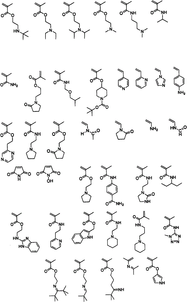
[0088] The structures of the monomers used in the synthesis of photoresist polymers along with their abbreviations are shown below:

[0089]

[0090] Synthesis of Poly(ECPMA / MCPMA / MNLMA / HADA)(PP-1)

[0091] The monomers ECPMA (5.092 g), MCPMA (10.967 g), MNLMA (15.661 g) and HADA (8.280 g) were dissolved in 60 g of propylene glycol monomethyl ether acetate (PGMEA). The monomer solution was degassed by bubbling nitrogen for 20 minutes. PGMEA (27.335 g) was added to a 500 mL three-neck flask equipped with a condenser and a mechanical stirrer, and degassed with nitrogen bubbling for 20 minutes. The solvent in the reaction flask was then warmed to 80°C. V601 (dimethyl 2,2-azobisisobutyrate) (0.858 g) was dissolved in 8 g of PGMEA, and the initiator solution was degassed with nitrogen gas bubbling for 20 minutes. The initiator solution was added to the reaction flask, and then the monomer solution was added dropwise to the r...


PUM


Abstract

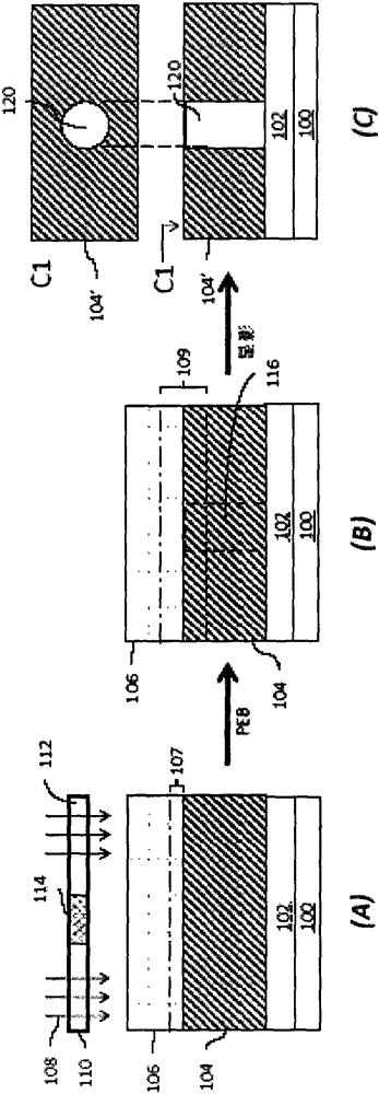
Methods of forming an electronic device, comprising in sequence: (a) providing a semiconductor substrate comprising one or more layers to be patterned; (b) forming a photoresist layer over the one or more layers to be patterned, wherein the photoresist layer is formed from a composition that comprises: a matrix polymer comprising a unit having an acid labile group; a photoacid generator; and an organic solvent; (c) coating a photoresist overcoat composition over the photoresist layer, wherein the overcoat composition comprises a quenching polymer and an organic solvent, wherein the quenching polymer comprises a unit having a basic moiety effective to neutralize acid generated by the photoacid generator in a surface region of photoresist layer; (d) exposing the photoresist layer to activating radiation; (e) heating the substrate in a post-exposure bake process; and (f) developing the exposed film with an organic solvent developer. The methods have particular applicability in the semiconductor manufacturing industry.

Description

Background technique [0001] The present invention generally relates to the manufacture of electronic devices. More particularly, the present invention relates to a photolithographic method and a photoresist protective layer composition that allow fine pattern formation using a negative tone development process. [0002] In the semiconductor manufacturing industry, photoresist materials are used to transfer images to one or more underlying layers deposited on a semiconductor substrate, such as metal, semiconductor, and dielectric layers, as well as the substrate itself. To increase the integration of semiconductor devices and allow the formation of structures with dimensions in the nanometer range, photoresists and photolithographic processing tools with high resolution capabilities have been and continue to be developed. [0003] Positive-tone chemically amplified photoresists are often used for high-resolution processes. Such resists generally employ a resin with an acid-la...

Claims


Application Information

Patent Timeline
Patent Type & Authority Applications(China)
IPC IPC(8): G03F7/00G03F7/11
CPCG03F7/16G03F7/20G03F7/38G03F7/0045G03F7/0392G03F7/0397G03F7/11G03F7/2041H01L21/0273G03F7/30
Inventor 朴钟根C·N·李C·安德斯李忠奉
Owner ROHM & HAAS ELECTRONICS MATERIALS LLC
Learn More