CIGS (Copper Indium Gallium Selenide)-based thin-film solar cell and manufacturing method thereof

A solar cell and manufacturing method technology, applied in circuits, photovoltaic power generation, electrical components, etc., can solve the problems of low efficiency, reduced conversion efficiency of thin-film solar cells, and reduced photoelectric conversion efficiency, so as to reduce production costs and reduce efficiency. , the effect of reducing reflections

Active Publication Date: 2015-11-04
厦门神科太阳能有限公司
View PDF4 Cites 6 Cited by
  • Summary
  • Abstract
  • Description
  • Claims
  • Application Information

AI Technical Summary

Problems solved by technology

[0007] Chinese patent CN101527332A discloses a CIGS-based thin-film solar cell, the solar cell structure is: Glass / Mo / CIGS / nCdS / nZnO / n+ZnO:Al, the thin-film solar cell can obtain higher photoelectric conversion efficiency, but If the thin-film solar cell is made into a solar cell module through a lamination process, its photoelectric conversion efficiency will decrease
The reason is that PVB, EVA, etc. are often used as adhesive layer materials for lamination. These adhesive layer materials contain a certain amount of water. After lamination, these water molecules will diffuse into the interior of thin-film solar cells, resulting in the failure of thin-film solar cells. drop in conversion efficiency
[0008] It can be seen that the efficiency of thin film batteries made by the above-mentioned existing preparation process is relatively low

Method used


Image

  • CIGS (Copper Indium Gallium Selenide)-based thin-film solar cell and manufacturing method thereof
  • CIGS (Copper Indium Gallium Selenide)-based thin-film solar cell and manufacturing method thereof
  • CIGS (Copper Indium Gallium Selenide)-based thin-film solar cell and manufacturing method thereof

Examples


Embodiment 1

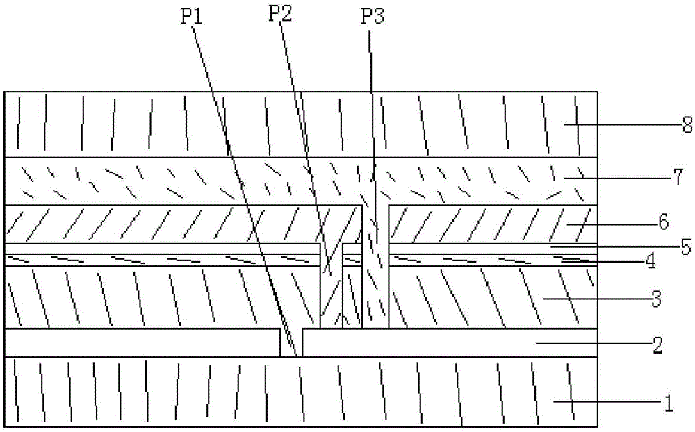
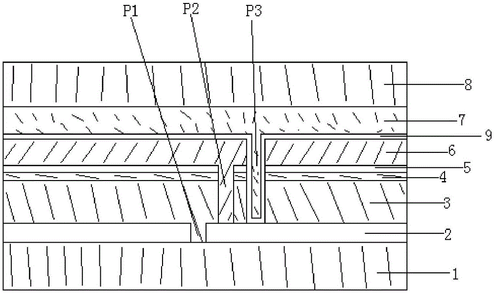
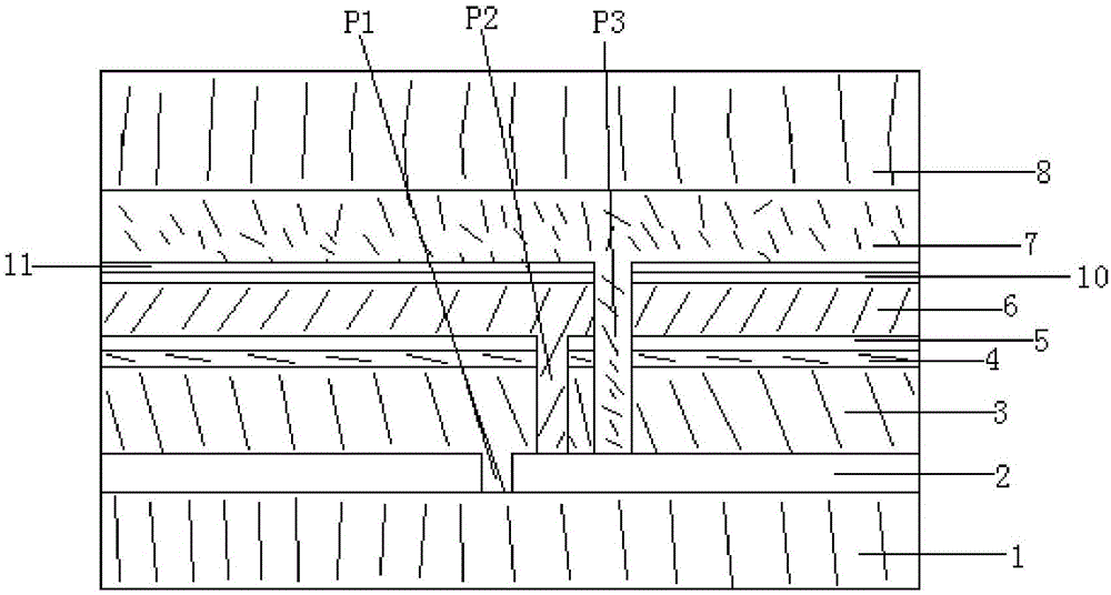
[0042] A 500nm metallic molybdenum electrode layer was deposited on a soda-lime glass substrate by magnetron sputtering; then a laser was used for P1 scribing; then a 2.0um thick copper indium gallium with a chalcopyrite structure was formed on the molybdenum electrode layer Diselenium light-absorbing layer; then, a 50nm CdS film was deposited on the light-absorbing layer by the chemical bath (CBD) method as a buffer layer; a 40nm intrinsic ZnO film was deposited on the buffer layer by magnetron sputtering; Needle for P2 scribing; then use magnetron sputtering to deposit 600nm AZO film layer on the intrinsic ZnO film layer; then use stylus for P3 scribing; then deposit 60nm aluminum oxynitride film layer on the AZO film layer , Si:Al=4:1 (atomic ratio) in the aluminum oxynitride film layer, the aluminum oxynitride silicon film layer only contains nitrogen on the side close to the AZO film layer, and the side far away from the AZO film layer One side only contains oxygen; then ...

Embodiment 2

[0045] A 550nm metal molybdenum electrode layer was deposited on a soda-lime glass substrate by magnetron sputtering; then a laser was used for P1 scribing; then a 2.0um thick copper indium gallium with a chalcopyrite structure was formed on the molybdenum electrode layer Diselenium light-absorbing layer; then, a 40nm CdS film was deposited on the light-absorbing layer by the chemical bath (CBD) method as a buffer layer; a 50nm intrinsic ZnO film was deposited on the buffer layer by magnetron sputtering; P2 scribing with a needle; then a 600nm AZO film layer deposited by magnetron sputtering on the intrinsic ZnO film layer; then P3 scribing with a stylus; and then a 20nm aluminum oxynitride silicon film layer deposited on the AZO film layer , Si:Al=9:1 (atomic ratio) in the aluminum oxynitride silicon film layer, N:O=9:1 (atomic ratio ), on the side away from the AZO film layer N:O=1:9 (atomic ratio); then PVB is used as the bonding material, and the thin-film solar cell and a...

Embodiment 3

[0048] A 550nm metallic molybdenum electrode layer was deposited on a soda-lime glass substrate by magnetron sputtering; then a laser was used for P1 scribing; then a 2.2um thick copper indium gallium with a chalcopyrite structure was formed on the molybdenum electrode layer Diselenium light-absorbing layer; then, a 40nm CdS film was deposited on the light-absorbing layer by the chemical bath (CBD) method as a buffer layer; a 50nm intrinsic ZnO film was deposited on the buffer layer by magnetron sputtering; Then use magnetron sputtering to deposit a 600nm AZO film layer on the intrinsic ZnO film layer; then use a stylus to perform P3 marking; then deposit a 200nm aluminum oxynitride film layer on the AZO film layer , Si:Al=49:1 (atomic ratio) in the aluminum oxynitride silicon film layer, N:O=4:1 (atomic ratio ), on the side away from the AZO film layer N:O=1:4 (atomic ratio); then PVB is used as the bonding material, and the thin-film solar cell and another clean ultra-white ...


PUM

PropertyMeasurementUnit
thicknessaaaaaaaaaa

Abstract

The invention provides a CIGS (Copper Indium Gallium Selenide)-based thin-film solar cell and a manufacturing method thereof. The CIGS-based thin-film solar cell comprises a substrate, a back electrode layer covering the surface of the substrate, a light absorption layer covering the back electrode layer, a buffer layer covering the light absorption layer, a transparent conducting layer covering the buffer layer, and an aluminum oxynitride silicon film layer covering the transparent conducting layer, or a composite film layer alternatively constructed by a zinc oxide silicon film layer and a silicon oxynitride film layer. Through the aluminum oxynitride silicon film layer or the composite film layer, external water molecules can be effectively prevented from entering the thin-film cell, and the decreasing degree of the efficiency of the thin-film solar cell is reduced. Meanwhile, an anti-reflection effect can be achieved, and the light absorption layer through which incident light reaches the cell is added, so that the short-circuit current of the thin-film cell can be increased.

Description

technical field [0001] The invention relates to the technical field of thin-film solar cells, in particular to a CIGS-based thin-film solar cell and a preparation method thereof. Background technique [0002] With the global warming, the deterioration of the ecological environment and the shortage of conventional energy, more and more countries have begun to vigorously develop solar energy utilization technology. Solar photovoltaic power generation is a zero-emission clean energy, which has the advantages of safety, reliability, no noise, no pollution, inexhaustible resources, short construction period, and long service life, so it has attracted much attention. Copper indium gallium selenide (CIGS) is a P-type semiconductor material with a direct band gap, and its absorption coefficient is as high as 105 / cm. A 2um thick copper indium gallium selenide film can absorb more than 90% of sunlight. The band gap of the CIGS thin film is continuously adjustable from 1.04eV to 1.67e...

Claims


Application Information

Patent Timeline
Patent Type & Authority Applications(China)
IPC IPC(8): H01L31/0216H01L31/032H01L31/18
CPCH01L31/02168H01L31/0322H01L31/18Y02E10/541Y02P70/50
Inventor 李艺明邓国云
Owner 厦门神科太阳能有限公司
Why Eureka
Try Eureka