Cigs-based thin film solar cell and preparation method thereof
A technology of solar cells and manufacturing methods, applied in the direction of circuits, photovoltaic power generation, electrical components, etc., can solve the problems of photoelectric conversion efficiency reduction, low efficiency, and conversion efficiency reduction of thin-film solar cells, so as to reduce efficiency reduction and reduce production costs , to reduce the effect of reflection
- Summary
- Abstract
- Description
- Claims
- Application Information
AI Technical Summary
Problems solved by technology
Method used
Image
Examples
Embodiment 1
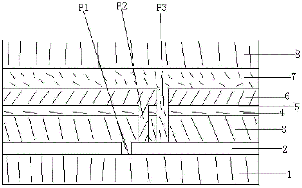
[0042] A 500nm metallic molybdenum electrode layer was deposited on a soda-lime glass substrate by magnetron sputtering; then a laser was used for P1 scribing; then a 2.0um thick copper indium gallium with a chalcopyrite structure was formed on the molybdenum electrode layer Diselenium light-absorbing layer; then, a 50nm CdS film was deposited on the light-absorbing layer by the chemical bath (CBD) method as a buffer layer; a 40nm intrinsic ZnO film was deposited on the buffer layer by magnetron sputtering; Needle for P2 scribing; then use magnetron sputtering to deposit 600nm AZO film layer on the intrinsic ZnO film layer; then use stylus for P3 scribing; then deposit 60nm aluminum oxynitride film layer on the AZO film layer , Si:Al=4:1 (atomic ratio) in the aluminum oxynitride film layer, the aluminum oxynitride silicon film layer only contains nitrogen on the side close to the AZO film layer, and the side far away from the AZO film layer One side only contains oxygen; then ...
Embodiment 2
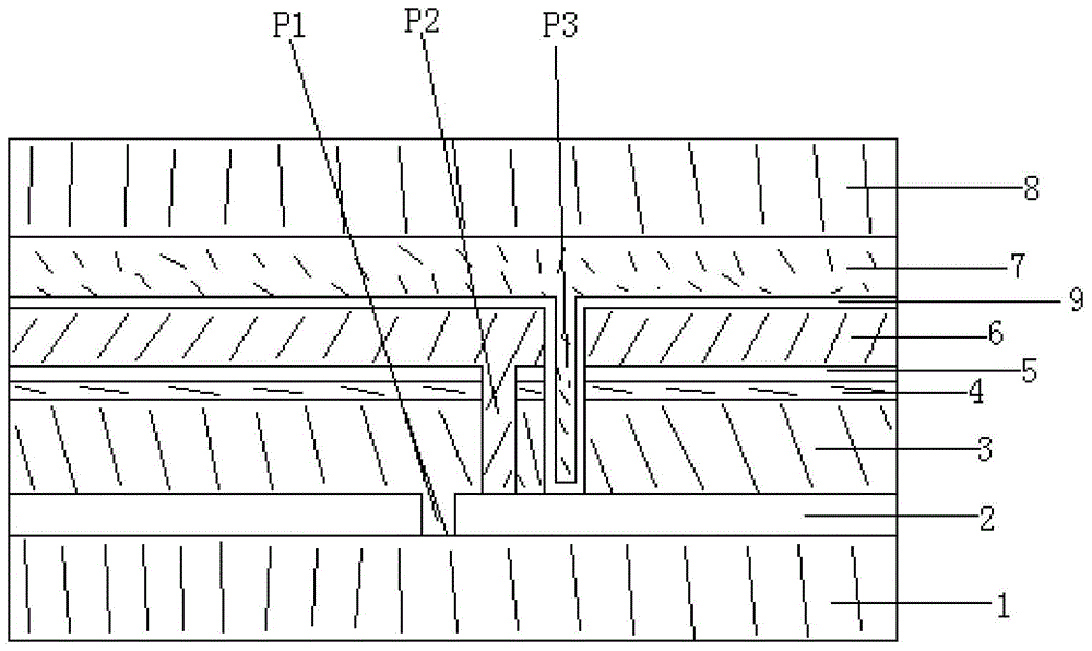
[0045] A 550nm metal molybdenum electrode layer was deposited on a soda-lime glass substrate by magnetron sputtering; then a laser was used for P1 scribing; then a 2.0um thick copper indium gallium with a chalcopyrite structure was formed on the molybdenum electrode layer Diselenium light-absorbing layer; then, a 40nm CdS film was deposited on the light-absorbing layer by the chemical bath (CBD) method as a buffer layer; a 50nm intrinsic ZnO film was deposited on the buffer layer by magnetron sputtering; P2 scribing with a needle; then a 600nm AZO film layer deposited by magnetron sputtering on the intrinsic ZnO film layer; then P3 scribing with a stylus; and then a 20nm aluminum oxynitride silicon film layer deposited on the AZO film layer , Si:Al=9:1 (atomic ratio) in the aluminum oxynitride silicon film layer, N:O=9:1 (atomic ratio ), on the side away from the AZO film layer N:O=1:9 (atomic ratio); then PVB is used as the bonding material, and the thin-film solar cell and a...
Embodiment 3
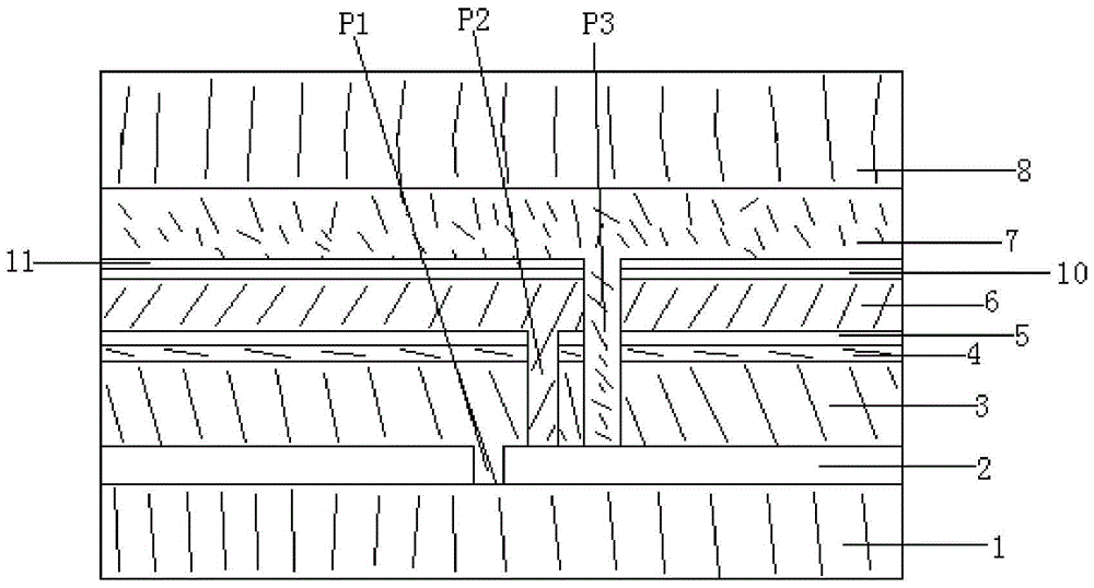
[0048] A 550nm metallic molybdenum electrode layer was deposited on a soda-lime glass substrate by magnetron sputtering; then a laser was used for P1 scribing; then a 2.2um thick copper indium gallium with a chalcopyrite structure was formed on the molybdenum electrode layer Diselenium light-absorbing layer; then, a 40nm CdS film was deposited on the light-absorbing layer by the chemical bath (CBD) method as a buffer layer; a 50nm intrinsic ZnO film was deposited on the buffer layer by magnetron sputtering; Then use magnetron sputtering to deposit a 600nm AZO film layer on the intrinsic ZnO film layer; then use a stylus to perform P3 marking; then deposit a 200nm aluminum oxynitride film layer on the AZO film layer , Si:Al=49:1 (atomic ratio) in the aluminum oxynitride silicon film layer, N:O=4:1 (atomic ratio ), on the side away from the AZO film layer N:O=1:4 (atomic ratio); then PVB is used as the bonding material, and the thin-film solar cell and another clean ultra-white ...
PUM
 Abstract
Description
Claims
Application Information


