
GaAs substrate mHEMT active region electrical isolating method

A technology of electrical isolation and active area, applied in the manufacturing of circuits, electrical components, semiconductor/solid-state devices, etc., can solve the problems of affecting the injection insulation resistance, deterioration of isolation performance, low resistivity, etc., to avoid mesa corrosion and Ion implantation, good repeatability, the effect of improving the implantation effect

Active Publication Date: 2015-11-18
GUILIN UNIV OF ELECTRONIC TECH
View PDF4 Cites 4 Cited by
  • Summary
  • Abstract
  • Description
  • Claims
  • Application Information

AI Technical Summary

Problems solved by technology

A large number of theoretical analysis and experimental results have shown that it is difficult to realize the ideal isolation of InGaAs / InAlAsm HEMTs on GaAs substrates only by ion implantation, because the lattice-matched InGaAs bandgap is only 0.74eV, and its The intrinsic resistivity is very small, and with the increase of the In composition, the InGaAs channel will be further narrowed, and the intrinsic resistance will be smaller; on the other hand, the activated ions form shallow donor energy levels in the material, which will also lead to isolation performance Third, the implanted ion concentration profile basically follows the Gaussian distribution law, and the peak value of its concentration is not on the surface, which will inevitably affect the injected insulation resistance of the extremely thin and highly doped InGaAs cap layer

Method used


Image

  • GaAs substrate mHEMT active region electrical isolating method
  • GaAs substrate mHEMT active region electrical isolating method
  • GaAs substrate mHEMT active region electrical isolating method

Examples


Embodiment Construction

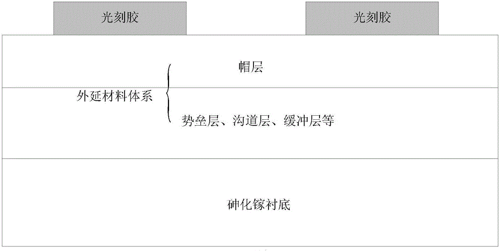
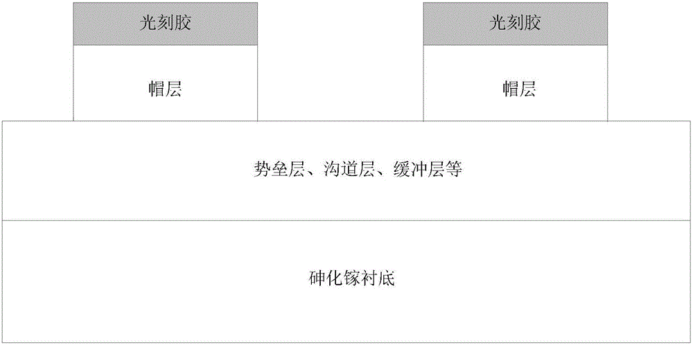
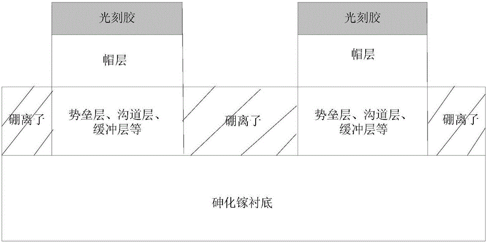
[0026] A gallium arsenide substrate mHEMT active region electrical isolation method, such as Figure 1-Figure 5 shown, including the following steps:

[0027] Step 1: Cleaning of device epitaxy samples.

[0028] Clean the sample, where the sample is an epitaxial material system with a variable composition multilayer structure grown on a gallium arsenide substrate, and the epitaxial material system includes a cap layer, a barrier layer, a channel layer and a buffer layer, etc., wherein the cap layer Layer is on top. The cap layer is a highly doped layer with a high doping concentration, which is conducive to forming an ohmic contact with the metal. In the present invention, the cap layer is 5nm In 0.53 Ga 0.47 As layer and 20nm In 0.65 Ga 0.35 As layer, the dopant is Si (silicon), the concentration is 10E+19cm -3 . The samples of variable composition multilayer structure epitaxial material system grown on gallium arsenide substrate can be obtained by MBE (molecular beam ...


PUM


Abstract

The invention discloses a GaAs substrate mHEMT active region electrical isolating method, which is a method combining wet etching and ion implantation for active region electrical isolation of a various-component high-electron-mobility transistor. The GaAs substrate mHEMT active region electrical isolating method comprises the steps of removing a surface highly-doped layer and then carrying out ion implantation isolation, thereby effectively improving the ion implantation effect, and further improving the isolation effect between active regions. Under the same condition, the isolating method combining ion implantation and mesa etching has the advantages of good electrical isolation effect, high process compatibility, small impact on subsequent process, good reproducibility, easy implementation and the like, effectively avoids the defects caused by adopting mesa etching and ion implantation separately, and has good use value for the semiconductor manufacturing process.

Description

technical field [0001] The invention relates to the technical field of semiconductor manufacturing, in particular to an electrical isolation method for an active region of a gallium arsenide substrate mHEMT (variable composition high electron mobility transistor). Background technique [0002] In the semiconductor manufacturing process, the main technical approaches for electrical isolation of active regions of compound semiconductor devices include: mesa corrosion isolation and implant isolation. [0003] The method of mesa etching to achieve electrical isolation has many disadvantages. For example, deep submicron grid bars are prone to broken bars when they span hundreds of nanometers of corrosion steps, which affects the yield; When the mesa sidewall is in contact with the conductive channel, the gate leakage current increases and the gate breakdown voltage decreases. There will be a certain amount of depletion when the chemical film is covered, which is also a problem t...

Claims


Application Information

Patent Timeline
Patent Type & Authority Applications(China)
IPC IPC(8): H01L21/762H01L21/306H01L21/265H01L29/778
CPCH01L21/2654H01L21/30612H01L21/7605H01L21/762H01L29/778
Inventor 李海鸥吉宪李琦高喜首照宇肖功利黄伟丁志华
Owner GUILIN UNIV OF ELECTRONIC TECH
Learn More