

High-medium single-layer miniature ceramic capacitor substrate material and preparation method thereof
A ceramic capacitor and high-dielectric single-layer technology, applied in the field of electronic information functional materials, can solve the problems of non-dense structure, unfriendly environment, poor material performance uniformity, etc., and achieve the effect of sufficient supply and low price
- Summary
- Abstract
- Description
- Claims
- Application Information
AI Technical Summary
Problems solved by technology
Method used
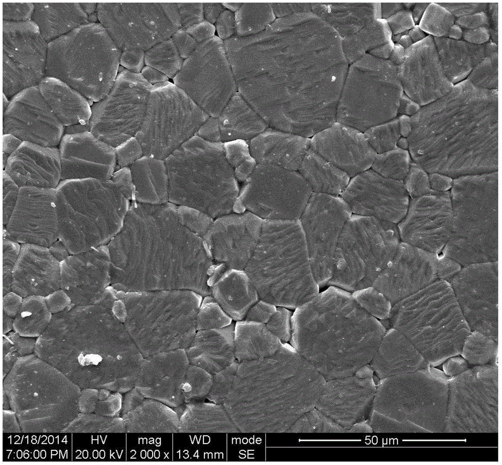
Image

Examples
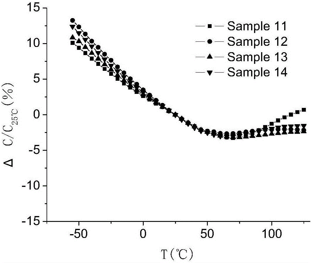
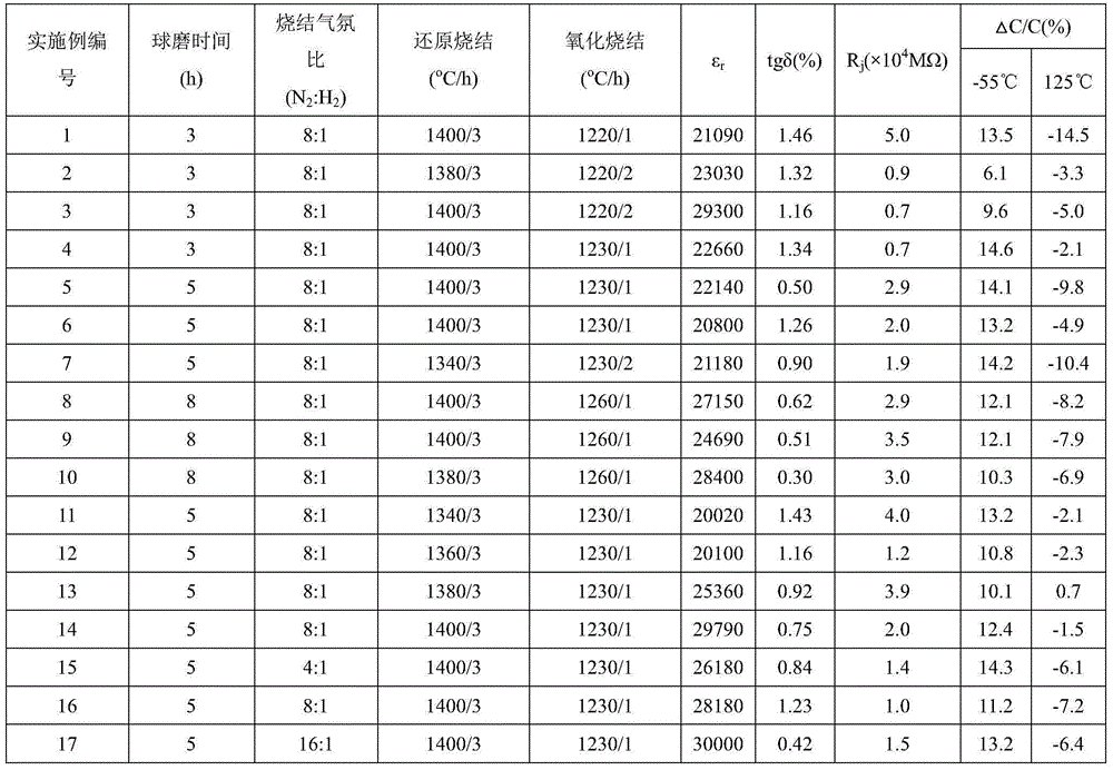
Embodiment 1~17
[0057] The preparation method of the above-mentioned high-dielectric single-layer micro-ceramic capacitor substrate material comprises the following steps:
[0058] (1.0) Preparation of composite oxide additive:
[0059] ①Select SrCO 3 , MnO 2 、TiO 2 , SiO 2 and B 2 o 3 As a raw material, prepare the material according to the above ratio, ball mill the prepared material with deionized water as the medium, dry it at 100°C-120°C and pass it through a 40-mesh sieve;
[0060] ②Dry and pass through a 40-mesh sieve, and pre-calcine the ball abrasive at 600°C-800°C for 1-2 hours to obtain the composite oxide additive powder.
[0061] (1.1) Ingredients
[0062] SrTiO 3 As the main material, add the above content of Nb respectively 2 o 5 , SiO 2 , Y 2 o 3 , CaSnO 3 and composite oxide additives are mixed to obtain a mixture;
[0063] (1.2) Ball mill
[0064] The mixture prepared in step 1.1 was ball milled, and after ball milling, the ball mill was dried at 120° C. and ...
PUM
 Abstract
Description
Claims
Application Information